Part Number: DS90CF384AQ-Q1
Hi Team,
Could you help provide the reference circuit for the device? Thank you.
Regards,
Roy
This thread has been locked.
If you have a related question, please click the "Ask a related question" button in the top right corner. The newly created question will be automatically linked to this question.
Part Number: DS90CF384AQ-Q1
Hi Team,
Could you help provide the reference circuit for the device? Thank you.
Regards,
Roy

Hi Roy,
Please use the schematics referenced in this previous E2E: DS90CF384A: documentation on
Best regards,
Ikram
Hi Roy,
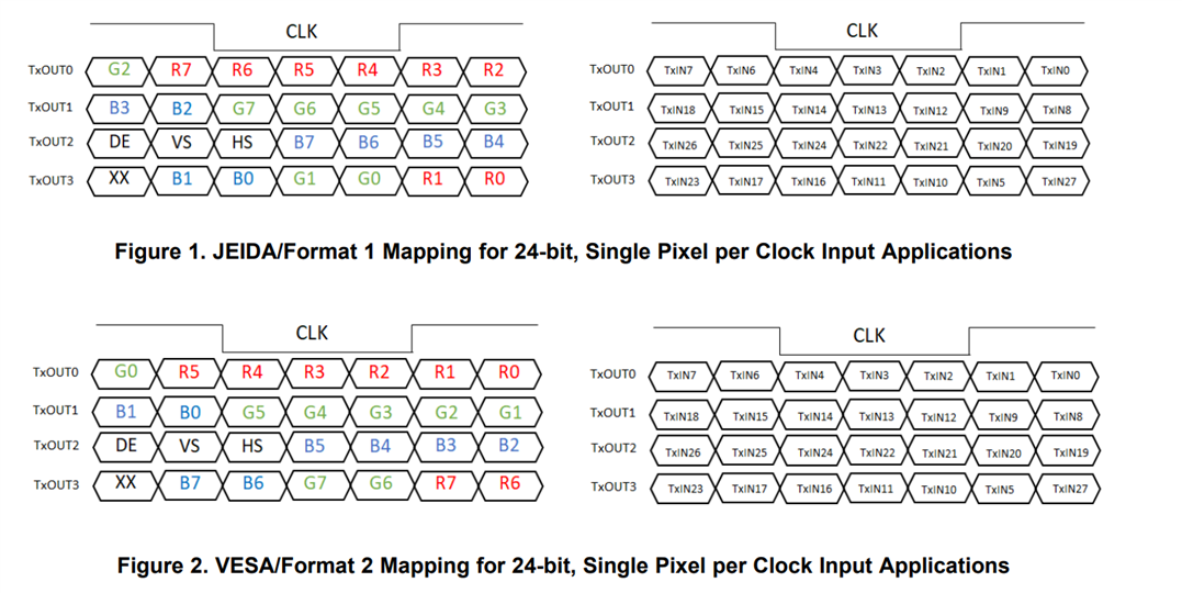
How the output RxOUT are connected to the RGB and HS/VS/DE pins depends on the incoming LVDS format.
There are two mapping formats for LVDS: VESA and JEIDA.
These formats are explained in this app note: https://www.ti.com/lit/an/snla014a/snla014a.pdf
Therefore, depending on the input LVDS format, the output will have to be connected accordingly.
For example,
Note that TxIN0 in this diagram would correspond to RxOUT0 on the DS90CF384AQ-Q1. Similarly the mapping for each RGB 0-8 can be found from this diagram based on the LVDS mapping from the source (serializer or LVDS video input from SoC).
Best regards,
Ikram