TDP158: OE pin

Part Number: TDP158
Other Parts Discussed in Thread: ESD224

Dear Technical Support Team,

I have an issue about OE pin.

I would like to send you the waveforms for the OE pin and power-up, either via email or through a private message on Friendship. I look forward to replying from you.

The measured voltage at the OE pin is approximately 2.275 V, as stated in the datasheet, which is below the datasheet’s VIH value of 2.31 V (Vcc=3.3V × 0.7).

As a result, some TDP158 devices function while others do not.

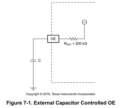
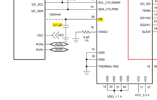
I have connected only a 0.1uF capacitor, exactly as specified in the datasheet.

When I measured the resistance between the OE pin and GND, it was approximately 203kohm, which is close to the 200kohm value listed in the datasheet.

I believe that for any device to function correctly, the voltage level at the OE pin must exceed VIH = 2.31V. 


Q1

Could you advise on how to resolve this issue?

Q2 

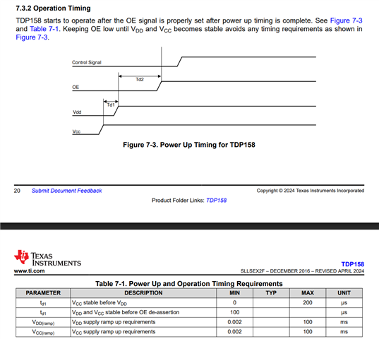
”Figure 7-1. External Capacitor Controlled OE” with external capacitor control, is the power supply connected to Rrst = 200 kohm in the internal circuit VCC = 3.3 V?


image.png

image.png

Best Regards,

ttd

  • TTD

    A passive reset circuit using an external capacitor and the internal pullup resistor will set DP158 OE pin properly. The VIH requirement does not applied toward the OE pin.

    The OE pin internally is being pulled up to 3.3V through the 200k resistor, but you will not see 3.3V on OE pin due to internal biasing. The 0.1uF pulldown capacitor is a recommendation, it needs to be tuned depending on the RC time constant delay (Tr) requirement in regard to power ramp up time.

    What is the exact issue you have with TDP158?

    Thanks

    David

  • Hi David,

    Thank you for your reply.

    I understand that the VIH requirements do not apply to OE.

    Among the Unexpected behavior units, there are some where the differential amplitude between the OUT_D1p/n and OUT_D2p/n pins is nearly zero.

    Note that the OUT_D0p/n and OUT_CLKp/n pins are outputting normally.

    Incidentally, even when an external High (3.3V) signal was applied to the OE pin of the defective unit, no output was generated.

    ・We verified 3 of TDP158 devices(abnormal), and regarding the output signals of the defective units,
     abnormal outputs occur on different output pins in each devices.
     Some units exhibited a differential amplitude of nearly 0 for all OUT_D[2:0] and OUT_CLK outputs.

    ・We conducted waveform comparison measurements between good and defective units on the DDC lines (SCL/SDA).
       When power was turned on with an HDMI monitor connected, the following differences in waveforms were observed between good and defective units for       SCL_SRC/SDA_SRC and SCL_SNK/SDA_SNK:

    OK unit:
       Confirmed that clock and data pulses are continuously output at normal voltage levels for approximately 40 ms.

    NG unit:
       Communication pulses cease immediately after a few clock cycles, or the signal voltage levels themselves are significantly
       unstable (failing to meet the specified High/Low levels).

    Question:

    Is there a register setting I can adjust to fix this, or anything else I should check?
    Is it possible that the connector side(OUT_D[2:0] and OUT_CLK) of the device is damaged?

    I sent schematic and waveform via private message on E2E.

    Could you check them?

    Best Regards,

    ttd

  • TTD

    1. Instead actively driving the OE pin, can they please remove the R397 to create a passive reset circuit? C169 can be tuned to meet the below power up timing requirement.

    2. EQ1 and EQ2 are both pulled low in the schematic, so they are providing minimal equalization. This needs to be tuned depending on the input channel insertion loss. But this will NOT impact the no output issue

    3. For the ESD they are using on the TDP158 output, the clamping voltage is too high which will not protect TDP158 output from potential ESD damage. We typically require clamping voltage at 8A Ipp IO to GND to be 4.5V or less. 

    • Can they do a TDP158 ABA swap to see if the issue follows the unit or the board?
    • Can they replace the current ESD diode with a lower clamping voltage ESD diode to see if the issue still duplicable?

    Thanks

    David

  • Hi David,

    Thank you for your reply.

    1. R397 is already unmounted, so attached power sequecnce waveform is only C169 =0.1uF for OE pin.

        Is this waveform satisfied power up timing requirement on datasheet?

    2.3 Thank you for your advice. I wiill check ABA swap and ESD diode protection.

    Best Regards,

    ttd

  • TTD

    1. R397 is already unmounted, so attached power sequecnce waveform is only C169 =0.1uF for OE pin.

        Is this waveform satisfied power up timing requirement on datasheet?

    There is a typo in the TDP158 datasheet, Td2 is VDD and VCC stable before OE de-assertion. 

    For Td2, we need to make sure OE can meet the min of 100us and this Td2 is controlled by the external pulldown capacitor on the OE pin.

    We need to use the scope to probe the OE along with VCC and VDD to check the Td2 timing, and right now the scope capture does not provide the OE pin timing.

    Thanks

    David 

  • Hi David,

    1.

    We need to use the scope to probe the OE along with VCC and VDD to check the Td2 timing, and right now the scope capture does not provide the OE pin timing.

    I already shared VCC and VDD and OE waveform. Is it enouch for you to see power up timing?

    Would it be sufficient to show, in the enlarged waveforms of VCC (ramp-up), VDD (ramp-up), and OE—specifically in the range of about 200 μs to 300 μs after VDD has stabilized—that OE remains at the low level for at least 100 μs?

    For Td2, we need to make sure OE can meet the min of 100us and this Td2 is controlled by the external pulldown capacitor on the OE pin.

    Is it necessary to maintain OE at 0.3 V or lower for at least 100 μs? Since the OE level rises gradually due to the CR, please specify the reference level.

    3.

    Do you have recomented ESD diode? I couldn't find it.

    ESD protection diodes product selection | TI.com

    For example, ESD224 is 8V clamping according to datasheet and app note.

    ESD Protection for HDMI Applications (Rev. A)

     We typically require clamping voltage at 8A Ipp IO to GND to be 4.5V or less. 

    Best Regards,

    ttd

  • TTD

    Looking at the ramp up timing waveform, can we delay the HDMI 5V ramp up after the TDP158 coming out of the reset?

    There are some 4-channel ESD diodes that can meet the clamping voltage requirement, but this will require a board re-design to change from the existing 1-channel ESD diode to the 4-channel ESD diode, would this work for them?

    Thanks

    David

  • Hi David,

    I understand that the HDMI 5V supply is ramped up after the OE reaches approximately 2.275V. What behavior is expected as a result of this? Is it to ensure a more reliable OE reset for output all channel correctly?

    Also, regarding the ESD diodes, since we are currently in mass production, we cannot make changes to the board immediately. For reference, could you please provide the part numbers of ESD protection components that meet the requirements?

    Best Regards,

    ttd

  • TTD

    I understand that the HDMI 5V supply is ramped up after the OE reaches approximately 2.275V. What behavior is expected as a result of this? Is it to ensure a more reliable OE reset for output all channel correctly?

    This is more a system design consideration. The HDMI sink will typically drive its HPD high as soon as the source provides HDMI 5V. You would like to have DP158 out of reset (OE pin high) and in normal operating mode before the HDMI sink drives the HPD high.

    For 4-channel ESD, please refer to Nexperia PUSB3FR4 as one example.

    Thanks

    David

  • Hi David,

    I understand the reason for delaying the 5V on the HDMI signal. Thank you also for the ESD example.

    To summarize our discussion so far: Is it correct understanding?

    ・Connecting only a 0.1uF capacitor to OE is in accordance with the recommended circuit in the datasheet, and
     the attached power sequencing (VDD, VCC, OE) is also fine except for the HDMI 5V.

    ・Among multiple TDP158 devices, there are individual variations in which channels do not output, but
     there is a possibility of damage caused by EOS, etc.
       

    Best Regards,

    ttd

  • TTD

    Your summary is correct. We should also do ABA swap to see if the issue follow the unit or the board.

    Thanks

    David

  • Hi David,

    Do you have TLP plots or data for TDP158?  Unfortunately, there is no deep snapback diode such as PUSB3FR4 in TI currently.

    ESD451: Protection for HDMI - Interface forum - Interface - TI E2E support forums

    Best Regards,

    ttd

  • TTD

    I do not have TLP plots or data for TDP158 pins.

    Thanks

    David