TDP142-Q1: Schematic and application review

Part Number: TDP142-Q1
Other Parts Discussed in Thread: TDP142
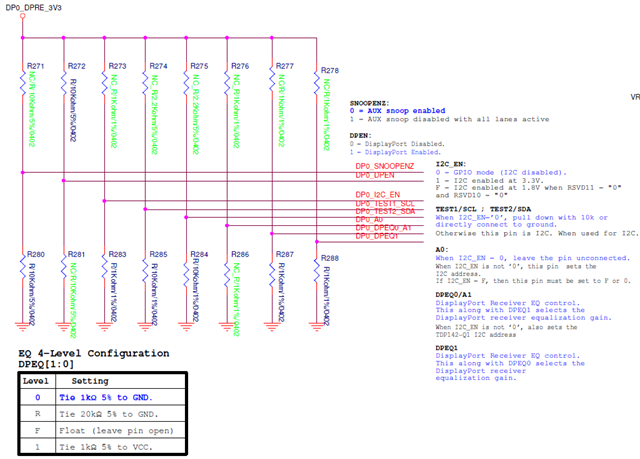
Hi Teams,

We are using the TDP142RGFRQ1 in our design. Please refer to the attached schematic and help review whether the connection architecture is correct.

Is this configuration considered a Source Application?

Also, could you please explain why the I2C lines are connected to the AUX channel?

In addition, could you clarify whether the Sink Application refers to a configuration where the signal enters from the left connector and exits from the right connector, similar to a dongle or adapter application?

Thanks.

TDP142RGFRQ1_20260624.pptx 

  • Hi,

    For the schematic review, please see my feedback below.

    1. Please provide the TDP142-Q1 configuration pin strapping setting

    2. The SP1004U-ULC-04UTG clamping voltage is too high, recommended clamping voltage is <=4.3V at Ipp of 8A. Recommend to use Nexperia PUSB3FR4 if possible.

    3. MUX0_AUX_P/N_A already has AC coupling and 100k PU/PD near the SoC side, please remove the duplicate set on the TDP142 schematic page

    4. How is DP0_OUT_AUXP/N being connected?

    5. Since MUX and TDP142 is AC coupled, please check and make sure the SoC DP output common mode voltage can meet the MUX common mode voltage requirement.

    Since this design uses a DP source connector and connect to a SoC, I would consider this to be a Source Side design. For sink side design, you would have a DP sink connector -> TDP142 -> Scalar.

    For I2C/AUX, I think you are referring to the DDC bus? This is to support DP++ implementation.

    Thanks

    David

  • Hi David,

    1. Please refer conf pin strapping as following.

    3. The DP connector pins 15/17 are connected to TDP142RGFRQ1 pins 16/17.

    For I2C/AUX, I think you are referring to the DDC bus? This is to support DP++ implementation

    => In our application, the I2C and AUX are not connected in the same way as in the source application. Could you please confirm whether this is acceptable?

    Thanks.

  • Hi,

    Also in the schematic, there should be 1M pull-down on CONFIG1 and 5M pull-down on CONFIG2.

    DPEQ0/1 need to be tuned depends on the TDP142 pre-channel and post-channel loss.

    The I2C and AUX are not connected in the same way as in the source application. Could you please confirm whether this is acceptable?

    I want to make sure there is no mis-communication, can you please highlight the connection in the block diagram or the schematic?

    Thanks

    David

  • Hi David,

    In our design, we do not have the connection shown by the blue lines in the figure below. In other words, AUX_P/N is not connected to the I2C lines.

    Could you please confirm whether this configuration is acceptable? Thanks.

  • Hi,

    The EVM is designed to support the implementation of a DP++ source. If the source in your source is not a DP++ source, then you will only need to use the AUX bus, and not the I2C or DDC bus. 

    Thanks

    David