Part Number: TXS0104E-Q1
Dear TI team,
I noticed a regression in a design with the TXS0104EQPWRQ1 voltage level translator. I'm asking you for confirmation on the observed behavior change and inputs on how to resolve the issue.
The marking of the old device is "04EQ1 16K C34E" and the marking on the new device is "04EQ1 TI 58K AX81".
The following schematic shows the use case of the device. It is used as a voltage translator for an SPI communication. Side A is at 1.8 V and is connected to a slave device with high impedance inputs and side B at 3.3 V with the master device, which drives the signals 1-3. We added an enable-logic linked to the LE signal because other slaves are on the MISO signal and the signals would create a short otherwise. There is no schematic change between the old and new boards.
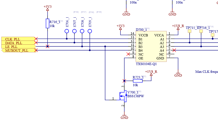
Problem description: with the new batch of voltage shifters, when a charge remains at the pin A3 due to a previous SPI command, starting a new command draws B3 low to select the slave and enable the voltage shifter but the voltage shifter creates a low-high edge on B3 (likely because of the remaining charge on A3 - no driving source is connected on that side), which leads to the voltage shifter to disable itself. This creates an enless loop of the voltage shifter enabling, creating a positive edge on B3 and then disabling itself again. This behavior cannot be observed with older voltage translator batches. To better understand what I'm describing here, let me add some measurements.
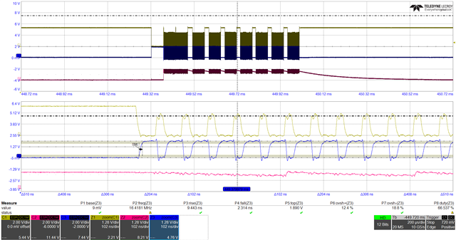
This image shows the old and expected behavior. Yellow is measured at B3, red is measured at A3 and blue is measured at OE. As you can see, the LE signal is driven low after a short break and this enables the voltage translator and after a short delay, it drives the A3 signal low.
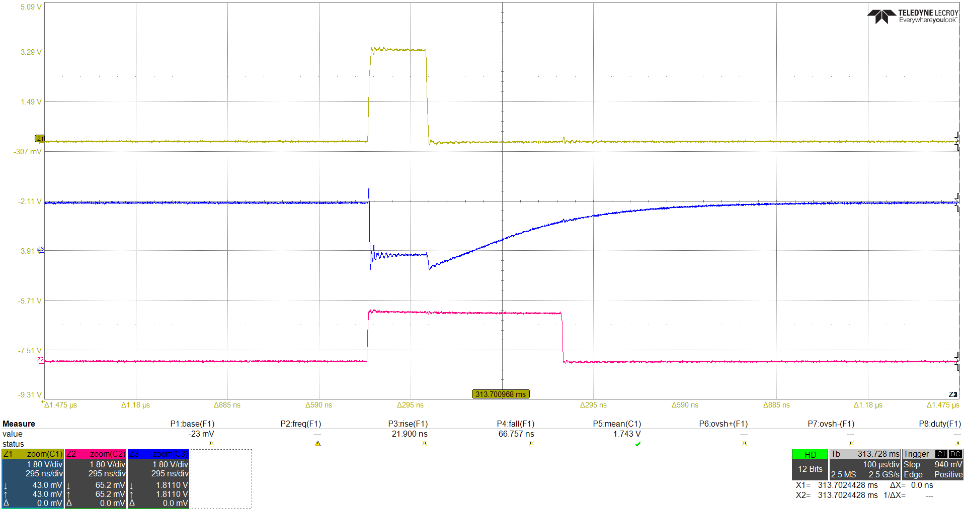
With the new batch of level translator the behavior is different. At the same point of the send sequence, driving LE on B3 low enables the voltage translator and at the point where the OE voltage is at around 1 V, the voltage translator forces the voltage on B3 high instead of pulling A3 low. This loop continues on indefinitely until the master drives the LE high again.
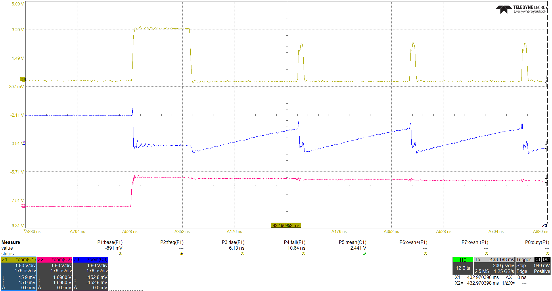
As already mentioned, the voltage on A3 is not driven by any source but is a remaining charge on the signal because both the SPI slave and the voltage translator inputs are high impedance (at least if the voltage translator is disabled). The only fix I can think of is to add a pull-down resistor on A3 but this is not recommended by your design documentation "Schematic Checklist - A Guide to Designing with Auto-Bidirectional Translators".
I am working on this issue since multiple days and was able to exclude other variables and the only one left is the voltage translator itself. Please help me with understanding this behavior and suggesting design improvements to fix this issue.
Thank you in advance for your assistance. Feel free to contact me in case more details are required.