This thread has been locked.

If you have a related question, please click the "Ask a related question" button in the top right corner. The newly created question will be automatically linked to this question.

DP83848VV driver

Hello 

I'm trying to run DP83848 eth with eCos greth driver. No matter what i write on MDIO registers, it always returns value of 0xFFFF when i read it back.

Since the MDIO registers always contain 0xFFFF, initialization process vails.

How the initialization process should be?

Best Regards,

_Gest_ 

  • This could be a problem with the board.  Could you provide a schematic for review?

    Patrick

  • I provide the schematic in the attachment here 3058.DP83848C.pdf

    Also regarding to this post : http://e2e.ti.com/support/interface/industrial_interface/f/142/t/196021.aspx

    --I have checked the  pins mentioned there. The only difference is that voltage of reserved pin 21 is 3.3V but pin 20 is just 3V.  

    --I also checked the other reserved pins(8-12). Each of them has voltage 3.3V, only pin 9 which has 1V. Is it a problem?

    --I get the same question with James Lim. In the datasheet it was mentioned that the PHYAD[0] has weak internal pull-up resistor, at what voltage this pin should be?

    Gest

  • Could you provide more detail on the measurements that you made?  Specifically, did you measure PFBIN1, PFBIN2, and PFBOUT on the package pins and confirm that the voltage is ~1.8V?  Similarly, did you measure RBIAS at the package pin and confirm that the voltage is ~1.2V? 

    In normal operation, the PHYAD0 / COL pin will be configured as an output and will drive the signal to ground or the supply.  In order to measure the value when the device is being strapped, you would need to probe the pin when the RESET_N pin is asserted.  In that case, the voltage will be determined as a resistor divider between the internal pull and any external resistance.  What is connected to the PHYAD0 / COL pin?  Is there a pull up resistor that is not shown in the schematic? 

    You mention that MDIO register accesses always read back 0xFFFF.  At what Phy address does the eCos greth driver expect to see the Phy?  Do you have the ability to read from different Phy addresses?  It is possible that the Phy has initialized at a different address from the one you are attempting to read.

    Patrick

  • I measured PFBIN1, PDBIN2, and PFBOUT pin, the voltage was 1,78 V. The RBIAS is 4,88k Ohm and the voltage accross it was 1,2 V.

    There is not any pull up resistor to PHYAD0/COL pin. I also leave the RESET_N pin floating. Are these critical??

    I found that the problem was in the phy addr configuration. I set pin configuration differently with the phy address defined in my FPGA. After fixing that issue, i could read and write the MDIO registers normally. I also checked the values of these registers and the values were as expected. But somehow, i still could not ping my board. The led blinked when i sent the ping but the software (eCos) was not seemed to receive anything from physical.

    _Gest_

  • The PFB and RBIAS measurements look good.

    Under normal circumstances it is not necessary to add a pull-up resistor to PHYAD0/COL and it is OK to leave the RESET_N pin floating. 

    Ping is an upper layer (above the OSI Physical layer) utility.  The fact that the FPGA does not receive the Ping does not necessarily mean that the Phy is operating incorrectly.  The Phy will not interpret the packet as a Ping packet and perform any filtering, but will simply receive it and pass it on.  Therefore, we will need to dig a little deeper to determine whether or not the Phy is operating correctly.

    The schematic would seem to suggest that you are operating in MII mode, but there is a header for selecting RMII mode.  Could you confirm that you are operating in MII mode?

    Are you generating the X1 reference clock with a crystal or with an oscillator?  Both are shown in the schematic. 

    Do you have the ability to transmit a packet from the FPGA? 

    Do you have the ability to probe the RX MII lines with an oscilloscope or a logic analyzer in order to evaluate the receive data (if any) coming out of the Phy?

    Patrick

  • Yes, the board operated in MII mode. I didn't connect the header, also double checked by measuring the MII mode and SNI mode pin and got 0 Volt. I use crystal to generate clock.

    I could not also send anything. I checked it with wireshark, the led indicated the same.

    I checked the RX_DV pin to indicate whether there was any valid data or not. Even when the led blinked, this pin was at zero volt.

    Basically i thought the software might be wrong. At initialization phase i just enabled auto negotiation and read some MDIO registers.

    Then i realized that after downloading the bitstream to the FPGA but my computer could not detect the greth (with the network manager). Just after downloading the program, my computer could connect to the board. From my experience with another greth phy, it is enough just download the bitstream to make my computer detect the greth.

    _Gest_

  • I would like you to evaluate the board without connecting to a link partner. 

    The first step in this process will be reading out the contents of the Phy registers.  Could you provide the full register contents?

    The second step in the process will be to evaluate the signaling on the board without a partner.  There will be two parts to this evaluation:

    1. Evaluate the signaling without a link.  For looking at output signaling, I generally use a short (1-2") pig-tail cable with 100 Ohm terminations.   I have attached a picture for reference.  With this cable plugged into the RJ-45 connector, the transmitter will be properly terminated and the voltage levels should be correct.  In this configuration, you can measure the transmit signaling.  I have also attached a picture showing the expected link pulse that should be measured. 
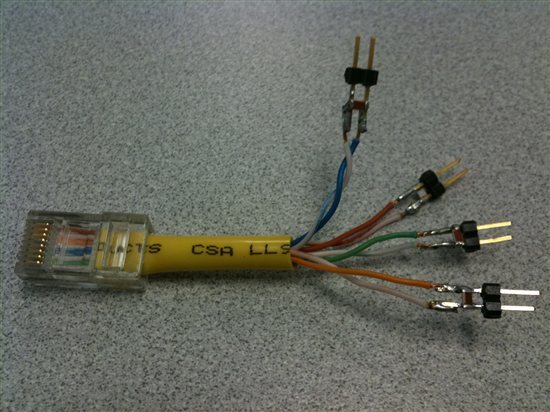
    2. Evaluate the signaling with the device linked to itself.  To allow the link to connect to itself, you will need to create an external loopback plug.  External loopback (also called "line loopback") can be used to loop the high speed lines of the link back to themselves.  The easiest way to achieve this is by making a custom cable and plugging it into the RJ45 connector.
        1. Cut a cable with about 1 foot of cable and the RJ45 connector
        2. Strip off about 3~4 inches of the outside plastic shield to expose the 4 pairs of twisted pair cable
        3. Bend back pairs 4/5 and 7/8 (these will not be used)
        4. Solder pair 1/2 to pair 3/6
              1. Solder wire 1 to wire 3
              2. Solder wire 2 to wire 6
        5. Now you have a loopback cable.
      Plug the cable into any operating 10/100 Ethernet port and link will be established (assuming Auto-Neg is enabled).  You can also force 100BASE-T or 10BASE-T full duplex to test those modes explicitly.  In this configuration, you can measure the transmit signaling.

    Once we have confirmed the device configuration by reviewing the registers and we have confirmed the baseline transmit signaling, we should have a good understanding of the functionality of the device.  If the device is functioning correctly, we can then move to the partner testing to determine what is happening with the partner.

    Patrick


    Pig-tail cable with 100 Ohm terminations:


    Link pulse waveform:

  • Here are all of the MDIO registers values when i connected it to partner link:

    FLAG MDIO reg 0 = 0x3100
    FLAG MDIO reg 1 = 0x7849
    FLAG MDIO reg 2 = 0x2000
    FLAG MDIO reg 3 = 0x5c90
    FLAG MDIO reg 4 = 0x1e1
    FLAG MDIO reg 5 = 0x0
    FLAG MDIO reg 6 = 0x7
    FLAG MDIO reg 7 = 0x2801
    FLAG MDIO reg 8 = 0x0
    FLAG MDIO reg 9 = 0x0
    FLAG MDIO reg 10 = 0x0
    FLAG MDIO reg 11 = 0x0
    FLAG MDIO reg 12 = 0x0
    FLAG MDIO reg 13 = 0x0
    FLAG MDIO reg 14 = 0x0
    FLAG MDIO reg 15 = 0x0
    FLAG MDIO reg 16 = 0x4800
    FLAG MDIO reg 17 = 0x0
    FLAG MDIO reg 18 = 0x2c00
    FLAG MDIO reg 19 = 0x0
    FLAG MDIO reg 20 = 0x10
    FLAG MDIO reg 21 = 0x0
    FLAG MDIO reg 22 = 0x100
    FLAG MDIO reg 23 = 0x1
    FLAG MDIO reg 24 = 0x0
    FLAG MDIO reg 25 = 0x8023
    FLAG MDIO reg 26 = 0x804
    FLAG MDIO reg 27 = 0x0
    FLAG MDIO reg 28 = 0x0
    FLAG MDIO reg 29 = 0x6011
    FLAG MDIO reg 30 = 0x3f
    FLAG MDIO reg 31 = 0x0

    Here are all of the MDIO registers values when i connected it to its own link (loopback line):

    FLAG MDIO reg 0 = 0x3100
    FLAG MDIO reg 1 = 0x7849
    FLAG MDIO reg 2 = 0x2000
    FLAG MDIO reg 3 = 0x5c90
    FLAG MDIO reg 4 = 0x1e1
    FLAG MDIO reg 5 = 0x0
    FLAG MDIO reg 6 = 0x4
    FLAG MDIO reg 7 = 0x2001
    FLAG MDIO reg 8 = 0x0
    FLAG MDIO reg 9 = 0x0
    FLAG MDIO reg 10 = 0x0
    FLAG MDIO reg 11 = 0x0
    FLAG MDIO reg 12 = 0x0
    FLAG MDIO reg 13 = 0x0
    FLAG MDIO reg 14 = 0x0
    FLAG MDIO reg 15 = 0x0
    FLAG MDIO reg 16 = 0x0
    FLAG MDIO reg 17 = 0x0
    FLAG MDIO reg 18 = 0x0
    FLAG MDIO reg 19 = 0x0
    FLAG MDIO reg 20 = 0x0
    FLAG MDIO reg 21 = 0x0
    FLAG MDIO reg 22 = 0x100
    FLAG MDIO reg 23 = 0x1
    FLAG MDIO reg 24 = 0x0
    FLAG MDIO reg 25 = 0x8023
    FLAG MDIO reg 26 = 0x804
    FLAG MDIO reg 27 = 0x0
    FLAG MDIO reg 28 = 0x0
    FLAG MDIO reg 29 = 0x6011
    FLAG MDIO reg 30 = 0x3f
    FLAG MDIO reg 31 = 0x0

    Also there was no signal detected by the oscilloscope. Even then led did not show any activity.

    Gest

  • One more question about the DP83848.

    What could be the reason that I have 3.3V on PFBOUT ?

    Grzegorz

  • Hello,

    It would be helpful if you could share  your schematic for review before before

    we debug your issue.

    Thanks,

    John