This thread has been locked.

If you have a related question, please click the "Ask a related question" button in the top right corner. The newly created question will be automatically linked to this question.

TFP410-EP Digital Transmitter

Other Parts Discussed in Thread: TFP410-EP, TFP410

Hello,

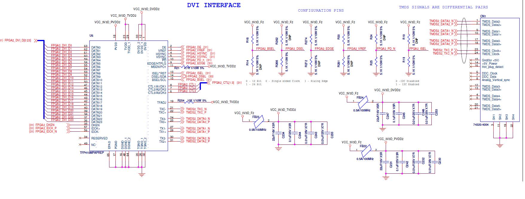
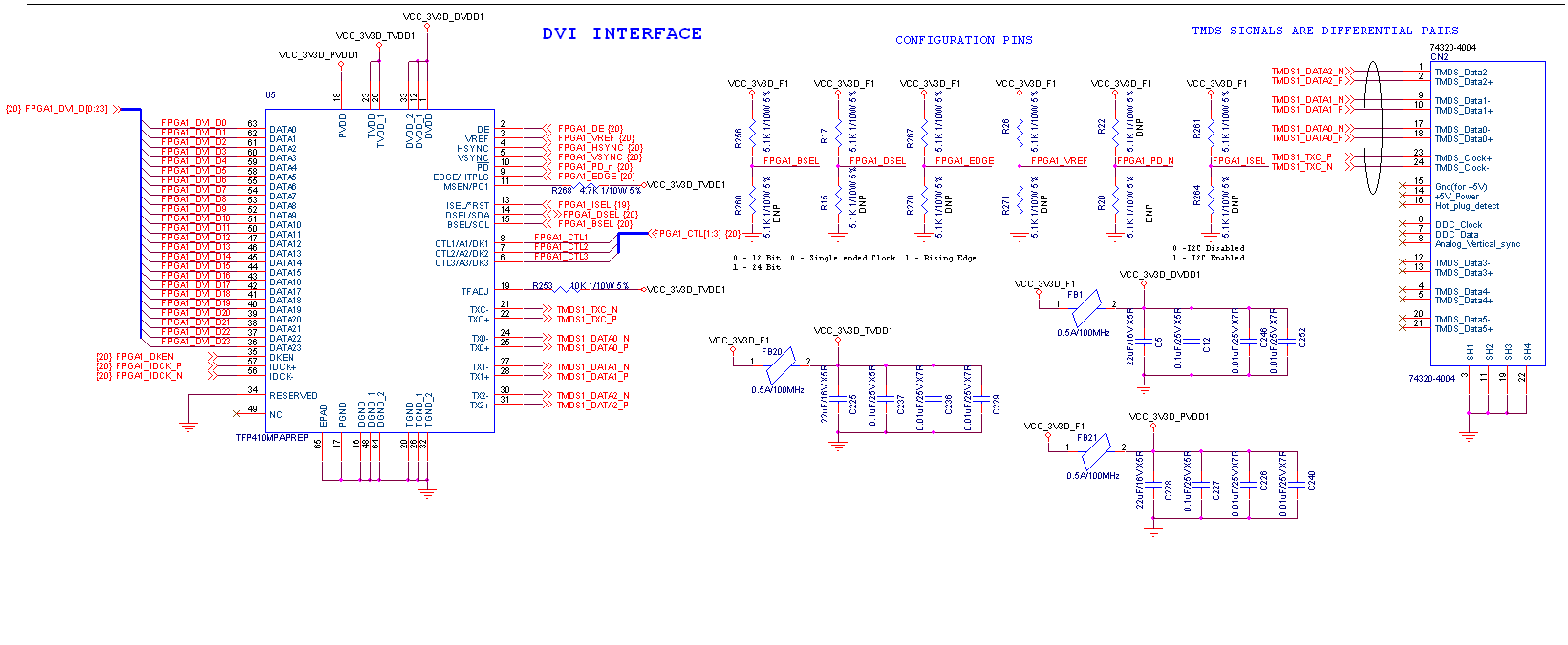
          In my project I am using TFP410-EP  Digital Transmitter, and I am interface this device with FPGA ,

I have gone through the data sheet as per my understanding I am thinking to do simple configuration using configurations pines and state pines.

can any one tell me answers of following 

1. How to interface / configuration TFP410-EP  with FPGA with out I2cinterface  ?

2. How to I configure or read the device ID, VenderID with out I2C interface?

3. how do I control the DE signal ? Vsync cound and Hsync count

  • Hello,

           We are reviewing your questions and We will reply soon.

    Regards,

    Diego.

  • Hello,

    You can drive the Data lines as well as the DE and SYNC directly from your FPGA.

    Regarding the VID and PID you will need the i2c lines.

    Regards.

  • Hello ,

           Thank Villeas for reply. you are correct and I am doing same!!

    Lets we first look at on DE, VSYNC, HYSNC. how to drive? In data sheet doesn't  any time diagram .I will be use monitor resolution 1920 * 1200, and my transmitting frequency is 100 mhz .

    can you tell me please how much time i will drive DE signal HIGH/LOW?

    how much time i will drive Vsync & Hsync signal HIGH/LOW?

  • Hello,

    DE should be high during the active video, this will be dictated by the number of pixels you are going to transmit, for example if you want to display a 1920x1200@60Hz plus the blanking time that resolution will give you a standard pixel clock of 193.25MHz. With a pixel time of 5.17ns, so you will need to keep DE asserted for (1920*5.17ns)=9.93us and then assert HSYNC and VSYNC should be asserted at every frame, i.e. if frame rate=60Hz then VSYNC period=16ms. The above numbers are raw calculations since the blanking period can change according with the display requirements.

    Keep in mind that the TFP410 supports a pixel clock up to 165MHz so the above resolution will not be supported.

    Regards.

  • Hello

           Do you have any development board of TFP410 . so I can interface fpga and  test my logic .. accordingly

    also plz see the EX of VGA .as like same thing how to calculate for DVI with respect to different parameters ..

  • Hello,

    We don't have a board like that right now (it is under development).

    I don't understand your question about  " see the EX of VGA .as like same thing how to calculate for DVI with respect to different parameters .."

    Can you elaborate more?

    Regards.

  • Hello ,

           Can you tell me please TFP410 chip support maximum DVI monitor resolution?

    Also in the data sheet Register DE_CET mention one formula "The value must be less than or equal to (2047 − DE_DLY)." what is this ?

    Also Chip configuration using I2c and all register setting is done so after that I need to do ISEL = 0 . ?

  • Hello,

    The TFP410 does not care about resolution, it only cares about Pixel Clock, the TFP410 supports a pixel clock up to 165MHz, this means that any resolution with a pixel clock within 165MHz is supported. An approximate formula to get the pixel clock is:  CLK=Horizontal_Lines x Vertical_Lines x Frame Rate

    So a resolution of 800x400@60 will have a pixel clock of approximately 19.2MHz plus blanking.

    DE_DLY is used to control the HSYNC timing when you use the DE Generator, if you are not using the DE Generator then DE_DLY is a don't care.

    In order to use the device in I2C mode you need to tie ISEL high.

    Regards.

  • Hello

                       Thanks for your reply

    Resolution :- This chip works maximum 165 Mhz  . if I used monitor 1920x1080@60 as per your calculation pixcel clock frequency is 182.5MHz.

                        so this pixcel frequency  > 165Mhz . Above resolution  wont be support ?

    DE-       yes I understand related to DE , but what is (2047 − DE_CNT).    / why you take only 2047 ?     

    ISEL-       yes you are correct if device is in I2c mode i need to tie ISEL high. but if configure all setting i need to make ISEL low ??


  • Hello,

    A resolution of 1920x1080@60 has a pixel clock of 148.5MHz per the VESA standard, so it will be supported by our device.

    DE_DLY is the number of pixels from when HSYNC is asserted to DE is asserted, 2047 is the maximum difference in lines that this device could support.

    Regards.

  • Hello Elias,

                    Thanks for your guide lines.. as per your input i wrote VHDL code for displaying white color on screen. Please find attached schematic of DVI interface with FPGA and VHDL code (you can open notepad++)  For 1920X1080 resolution  I am doing generation of Hsync ,  Vsync, DE timing at pixcle clock of 147.22mhz (actually it should 148.5mhz ) and sending 24 bit data on DVI line .

     I am using this mode- 24 bit single ended , rising edge clock.

    A1A2A3 = 101; -----Default

    BSEL= High---24-bit input, single-edge input mode.

    DSEL= HIgh

    Dken= High

    Edge= High;--- high level selects the primary latch to occur on the rising edge of
    the input clock IDCK+.

    ISEL/RSTn= low ---I2c Disable

    PDn= High ;

    IDCK+.=147.22Mhz

    IDCK- ='0'

    *********************** VHDL CODE**********************************************

    --------------------------------------------------------------------------------
    -- DVI_top.vhd
    --
    -- Digital video INTERFACE color bar generator
    --
    --
    --
    --
    --------------------------------------------------------------------------------
    --

    library ieee;
    use ieee.std_logic_1164.all;
    use ieee.std_logic_unsigned.all;
    --use ieee.std_logic_arith.all;
    use ieee.numeric_std.all;
    Library UNISIM;
    use UNISIM.vcomponents.all;

    entity DVI_top is
            generic (
                image_width_i   : integer   := 1920;         --- 640 FOR 1280X1024
                sig_hsync : integer :=88;                  --- 56 FOR 1280X1024
                hbporch : integer :=  148;               --- 70 FOR 1280X1024
                sig_hfproch : integer := 88;                --- 12 FOR 1280X1024
                image_height_i   : integer   := 1080;        --- 1024 FOR 1280X1024
                sig_Vsync : integer := 5;                   --- 3 FOR 1280X1024
                sig_VBproch : integer := 36;                --- 38FOR 1280X1024
                sig_VFproch : integer := 4  ;                --- 1 FOR 1280X1024
               DATA_width        : integer   := 8
            );
        port (
              sys_clk_i            :in  std_logic;                                 -- clock input
              sys_rst_i            :in  std_logic;                                 -- async reset input
              dvi_data_o         :out std_logic_vector(23 downto 0);           -- video output
              dvi_h_sync_o        :out std_logic;                                 -- horizontal sync out
              dvi_v_sync_o        :out std_logic;                                 -- vertical sync out
              dvi_DE_o           :out std_ulogic ;                            
              dvi_clk_p_o        :out std_logic ;
              dvi_clk_n_o        :out std_logic ;
              dvi_CTL_o       :out std_logic_vector(2 downto 0)

      );
    end DVI_top;

       architecture Behavioral of DVI_top is


        COMPONENT dcm_dvi
        PORT(
            CLKIN1_IN : IN std_logic;
            RST_IN : IN std_logic;          
            CLKOUT0_OUT : OUT std_logic;
    --        CLKOUT1_OUT : OUT std_logic;
            LOCKED_OUT : OUT std_logic
            );
        END COMPONENT;    


        signal LOCKED  :std_logic ;
        signal RSTn : std_logic ;
        signal pixelcount_sig        : std_logic_vector(15 downto 0);
        signal linecount_sig       : std_logic_vector(15 downto 0);
        signal testpattern_sig : std_logic_vector(23 downto 0);
        signal testpat_wrreq_sig  : std_logic;
        signal white_sig  :integer;
        signal yellow_sig : integer;
        signal cyan_sig : integer;
        signal green_sig: integer;
        signal magenta_sig: integer;
        signal red_sig: integer;
        signal blue_sig: integer;
        signal black_sig : integer;
        signal nonactive : integer  ;
        signal sig_hbporch : integer  ;
        signal DATA_byte_reg_i : integer  := 4;
        signal testenable : std_logic;
        signal hsync_sig: std_logic;
        signal vsync_sig: std_logic;
        signal hfull_sig: std_logic;
        signal vfull_sig : std_logic;
        signal start,sig1 : std_logic;
        signal dvi_clk : std_logic;
        signal rd_en : std_logic;
        signal sig_ena :  STD_LOGIC;
        signal sig_wea :  STD_LOGIC_VECTOR(0 DOWNTO 0);
        signal sig_addra :  STD_LOGIC_VECTOR(15 DOWNTO 0);
        signal sig_dina :  STD_LOGIC_VECTOR(23 DOWNTO 0);
        signal data_in : std_logic_vector(23 downto 0)  := (others=>'0') ;
        signal wr_addra :  std_logic_vector(4 DOWNTO 0):= (others=>'0') ;
        signal rd_addrb :  std_logic_vector(4 DOWNTO 0):= (others=>'0');


    begin

        dcm_dvi_clk: dcm_dvi PORT MAP(
            CLKIN1_IN => sys_clk_i     ,
            RST_IN => not sys_rst_i    ,
            CLKOUT0_OUT => dvi_clk , -- 147.22 mhz
    --        CLKOUT1_OUT =>clk_54mhz , --- 53.33 mhz
            LOCKED_OUT => LOCKED
        );
        
    dvi_clk_p_o <= dvi_clk;
    dvi_clk_n_o <= '0';
    RSTn   <= LOCKED;
    dvi_CTL_o   <=  "101";


    process(RSTn,dvi_clk)
    begin
      if(RSTn = '0') then
        sig1 <= '0';
        rd_addrb <= (others => '0');
      elsif (rising_edge(dvi_clk)) then
           if  ( rd_en  ='1' and testpat_wrreq_sig = '1' )then    
                  rd_addrb <= rd_addrb + '1';
              elsif (  testpat_wrreq_sig = '0') then
                rd_addrb <= (others => '0');
              end if;
                end if;
    end process;  ----------------------


    --  ---------------- vedio Hsync,Vsync,DE gen ---------
       process(RSTn,dvi_clk)
    begin
      if(RSTn = '0') then
        pixelcount_sig <= (others => '0');
      elsif (rising_edge(dvi_clk)) then
        if (pixelcount_sig=(image_width_i+sig_hbporch+sig_hfproch)-1)then
           pixelcount_sig <= (others => '0');
        else
          pixelcount_sig <= pixelcount_sig + '1';
        end if;
       end if;
    end process;


    testpat_wrreq_sig <= '1'     when ((pixelcount_sig > sig_hbporch)and (pixelcount_sig <=(image_width_i+sig_hbporch))) else '0';
    hsync_sig <= '1' when ((pixelcount_sig > (sig_hsync-1)) and (pixelcount_sig <= (image_width_i+sig_hbporch+sig_hfproch)-1))else '0';


    dvi_h_sync_o<=  hsync_sig;

    dvi_DE_o <= testpat_wrreq_sig;

    sig_hbporch <= sig_hsync + hbporch ;

    nonactive <= sig_hbporch-1;


    --------------------------------------------------------------------------------
    --Line counter and Vsync
    --------------------------------------------------------------------------------

    process(RSTn,dvi_clk)
    begin
      if(RSTn = '0') then
        linecount_sig <= (others => '0');
      elsif rising_edge(dvi_clk) then
        if (linecount_sig=(image_height_i+sig_Vsync+sig_VBproch+sig_VFproch)-1)then
           linecount_sig <= (others => '0');         --linecount_sig;
        elsif(pixelcount_sig=(image_width_i+sig_hbporch+sig_hfproch)-1)then
          linecount_sig <= linecount_sig + '1';
        end if;
      end if;
    end process;

    vsync_sig <= '1' when ((linecount_sig> (sig_Vsync-1)) and (linecount_sig<= (image_height_i+sig_Vsync+sig_VBproch+sig_VFproch)-1))else '0';

    dvi_v_sync_o <=   vsync_sig;  ---


    dvi_data_o <= "FFFFFF"    ;                


    end Behavioral;

    Can i know with this code i will get white screen on DVI monitor..    0537.DVI_top.doc

  • Hello,

    Your schematic shows PD# connected to ground, this terminals should be connected to 3.3V when the I2C mode is disable.

    All other connections looks correct.

    Regards.

  • Hello Elias,

                    Thanks for your reply . So I can directly give 24 bit RGB data along with Hsync,Vsync, and DE signal.

    So i don't need any DVI driver ?

  • Correct,

    The TFP410 will output TMDS signals that can be directly connected to a DVI receiver.

    Regards.

  • Hello ELIAS,

     As per above all discussions i am trying to communicated with this chip , but i am not getting any out put signs from the chip..I think chip is in reset ..

    can you tell me please where I am wrong.

    Can you please provide me your contact no as well as your free time , so we can talk on phone

  • Check the PD# signal.

    When the i2c interface is disable the PD# terminal must be tied to 3.3V.

    When the i2c interface is enable the PD# signal defaults to 0 and you have to write a 1 on the PD bit (Register CTL_1_MODE, page 18 of Datasheet)

    Regards.

  • Hello ELIAS,

    Yes PD# signal is connected to ground only.

    Also i  enabled i2c for reading vender ID but i could not able to read the vender id.. always getting 00 from the device ...

    one question

    when CTL = "000" 

    device address /chip address  = 0111000 (if i consider 7 bit) and LSB bit will 0/1 for write/read?

    And when i power on the board i saw all the control signals shows 3.3v  .. can i know by default what will be voltage level of all control pins 

  • You are probably not reading from the correct address.

    At every power-up cycle, the i2c interface must be rest, it is recommended to connect the terminal ISEL to the system Rest which is low until all power supplies are stable.

    Try reading from different addresses, maybe the device is latching the CTL high because of the above condition.

    Regards.

  • Hello

    Can you tell me please what will be I2C clock frequency for reading and writing registers

  • The frequency is 100kHz.

    Regards.

  • Hello ,

    Thanks  ,I tried to I2C for reading the Device ID from Chip, but I am getting always got FF from Chip,as per data sheet i am expected 014C (if I wrote address 00 and 01)..

    Also I tried Without I2c I am not getting anything out of chip..

    please the the below  without I2c  configuration

       
    dvi_clk_p_o <= dvi_clk; ----148mhz
    dvi_clk_n_o <= '0';       ----
    dvi_ISEL_o <=  '0';  
    dvi_BSEL_o <=  '1';
    dvi_EDGE_o <=  '1';
    dvi_DSEL_o <=  '1';
    dvi_VREF_0 <=  '1';
    dvi_CTL_o   <=  "100";  --defualt
    dvi_PD_n_o <=  '1';
    dvi_DKEN_o <=  '1';

    can you tell me where I am going wrong ...

  • Your hardware configuration seems correct.

    You have to put a 50ohm resistor to ground on every TMDS output in order to measure a voltage.

    Regards. 

  • Hello Elias,

                           Thank you very much for your Inputs .,  I am able to configure the TFP-410 chip,

    My one problem was i am not connecting DVI cable from monitor , so because of that MSEL pin always low, once I connected  the monitor DVI cable, then I saw MSEL going High, Differential data is toggling

    Another problem was setting the DKE[3-1]-pins, as per my pixel clock frequency.

    Once again thank you very much..

  • Hello Elias,

                     I am facing one more problem when I am trying to read Device ID i am always getting FF ..

    By Using I2C I am not able to configure DVI chip, Can you tell me please what are register values i need to write

    Register ,08, 09, 0A

    I am using external DE.,

    Please see the attached my schematic

    on Board signal/Pin status 

    PD = open ,

    ISEL/RST = Pullup,

    DSEL/SDA = Pullup

    BSEL/SCL = pullup,

    MSEN/PO1 = pullup,

    EDGE = pullup,

    we not using hot plug detection. 

  • Hello,

    Use the base address 0x7E and add an offset according with each "SUB-ADDRESS" listed on the datasheet, in this way if you want to read the DEV_ID (sub-addr=02) you will have to read the address 0x80.The i2c interface only supports 8-bit transactions.

    Connect PD to 3.3V, make sure Vref is within 0.55V-0.9V.

    Connect ISEL=BSEL=DK1=DK2=DK3=3.3V

    Connect DSEL=0V

    When entering in i2c mode the device defaults to power-down mode, so the first thing to do is to write a "1" to bit0 of the sub-address 0x08, after that the value you will write to sub-address 08,09 and 0A depends on your configuration according with Table 1 in the datasheet.