This thread has been locked.

If you have a related question, please click the "Ask a related question" button in the top right corner. The newly created question will be automatically linked to this question.

RS-485 transceiver input output protection

Hi,

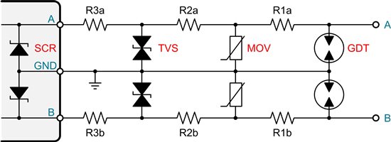
Application note SLYT484 suggests on page 6 a TVS application circuit for overvoltage protection. Series resistors R1 and R2 are between the junction TVS - line and the transceiver. Is it correct?  I would expect to have the resistors between the line and junction TVS - transceiver so that they would limit overcurrent to both the TVS and transceiver. Overvoltage is limited by the TVS anyway.

Could you please let me know why you connect it in this way and if there are any benefits of such wiring.
We would prefer to connect R1 and R2 as we described. Is it possible?

Thank you

Daniel

4111.SLYT484 (page_6).pdf


  • Hey Daniel!

    The issue arises when the clamping voltage of the internal ESD structure is lower than the clamping voltage of the external protection device. When this happens the device will shunt all the energy and the external TVS diode will not remain on. This can result in damage to the ESD cell. With the series resistor in place there will be a voltage drop between the TVS diode and the internal ESD structure of the device. This will allow the external TVS diode to remain on during the transient event and clamp the voltage and protect the device from the transient more effectively.

    This external TVS diodes are usually rated for 30W to more of peak power dissipation, and are built to handle ESD, EFT and surge events.

    Thanks,

    John

  • Here is a 3-stage transient protection scheme. Each protection device has a firing or break-down voltage where it starts conducting, and a higher clamping voltage at which it fully conducts. The general principle is that the weaker device of the next stage has a clamping voltage that is lower than the breakdown voltage of the previous device. Therefore in order to keep the previous or stronger device turned on, a series resistor is implemented to maintain the necessary voltage drop.

    So for example, the voltage drop across R1a plus the clamping voltage of the MOV must be equal to the clamping voltage of the GDT (and therefore greater than its firing voltage.

    the same procedure is applied to all following stages so that the drop across R3a and the clamping voltage of the transceiver internal SCR match the clamping voltage of the TVS.

    Hope this clarifies it. Regards, Thomas