This thread has been locked.

If you have a related question, please click the "Ask a related question" button in the top right corner. The newly created question will be automatically linked to this question.

SN65DSI83-Q1: SN65DSI83-Q1 can not display, 0xE5 register data is 0x09

Part Number: SN65DSI83-Q1

Dears, 

I am the FAE of MarubunArrow7268.DSI83-Q1 problem.xlsx

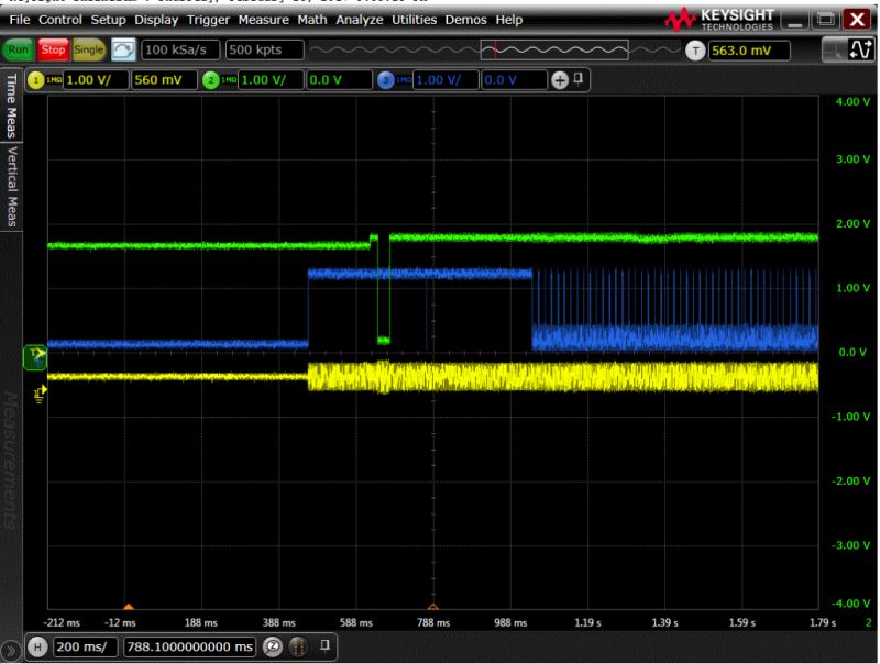
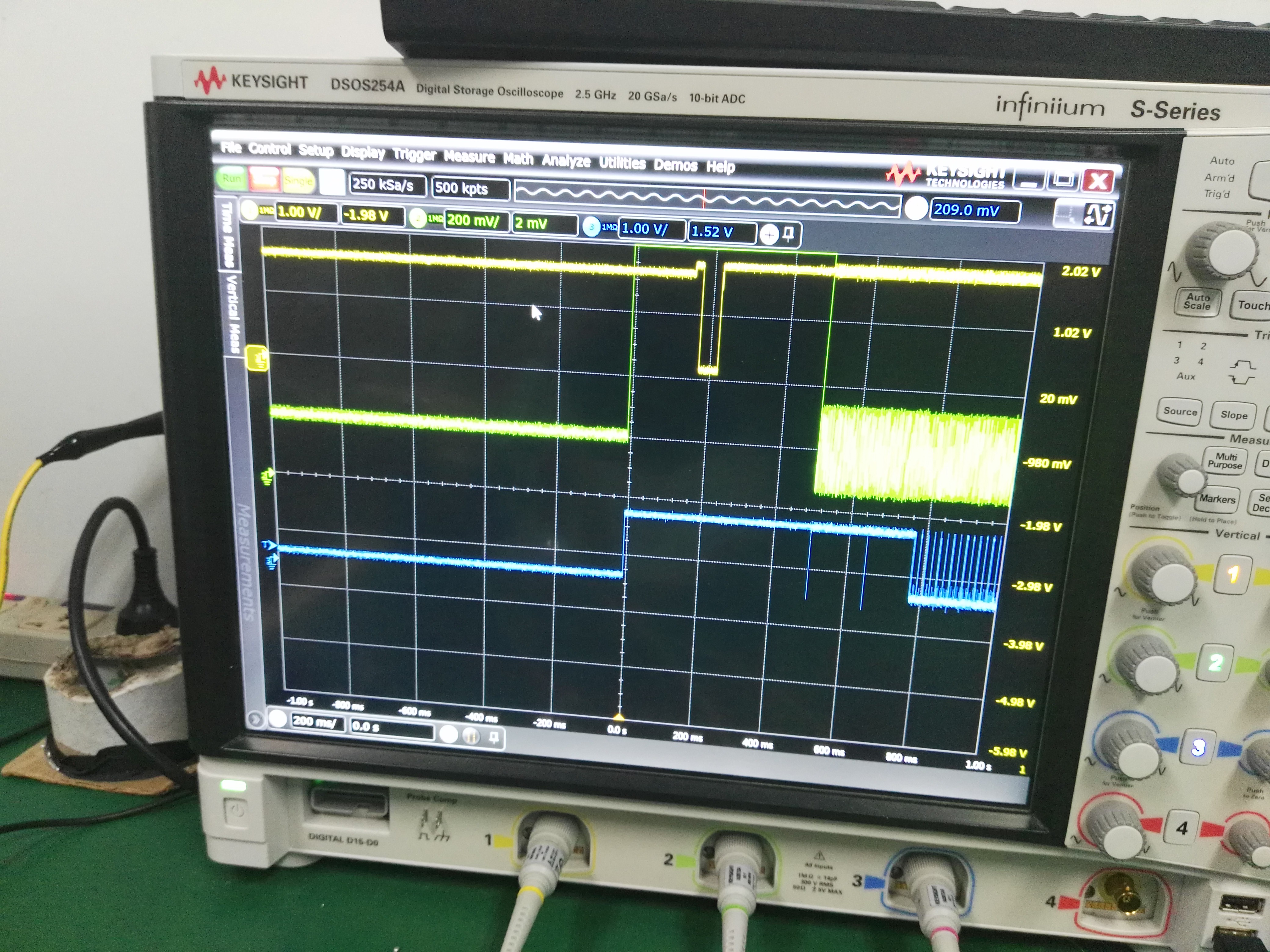
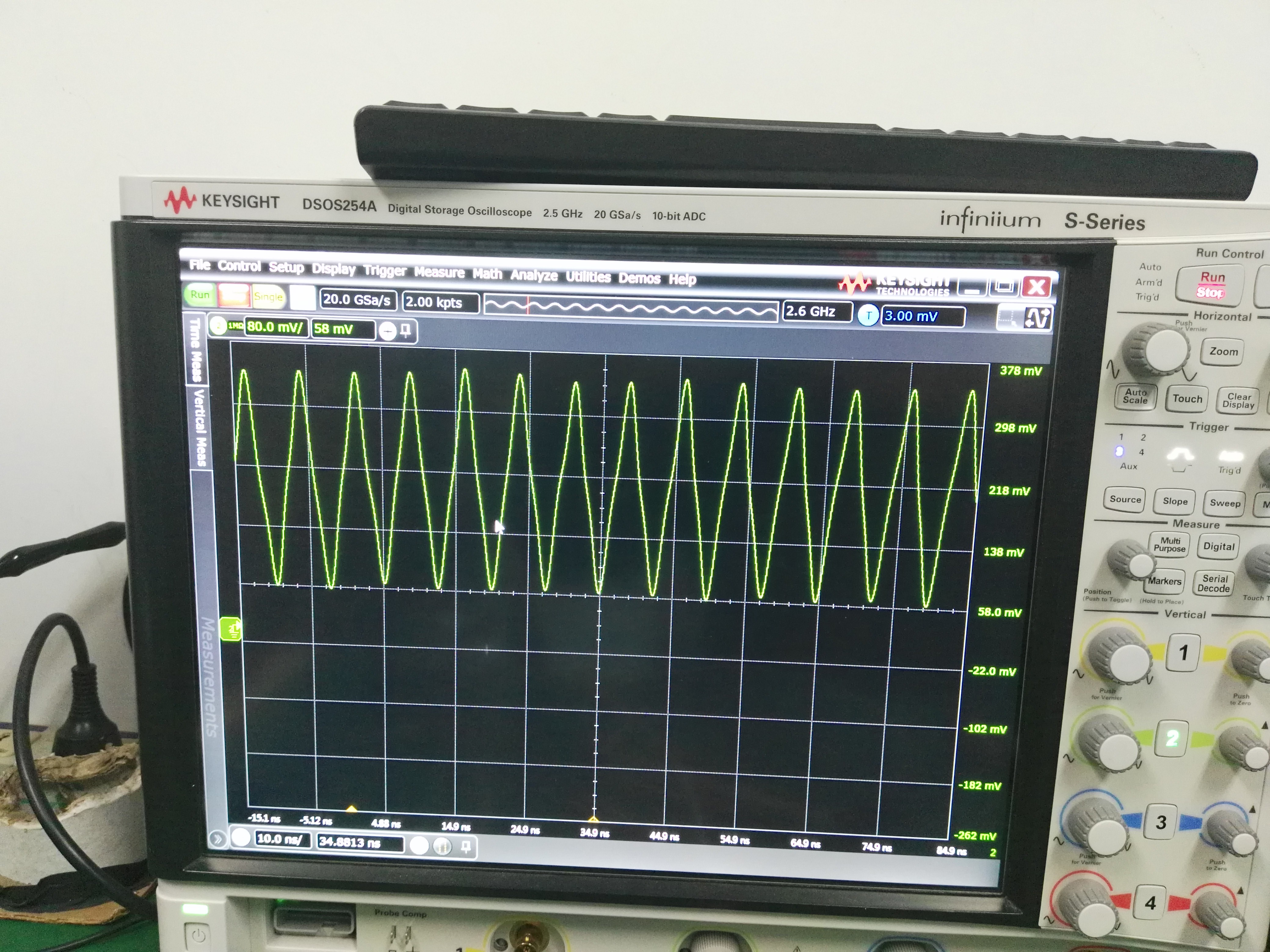
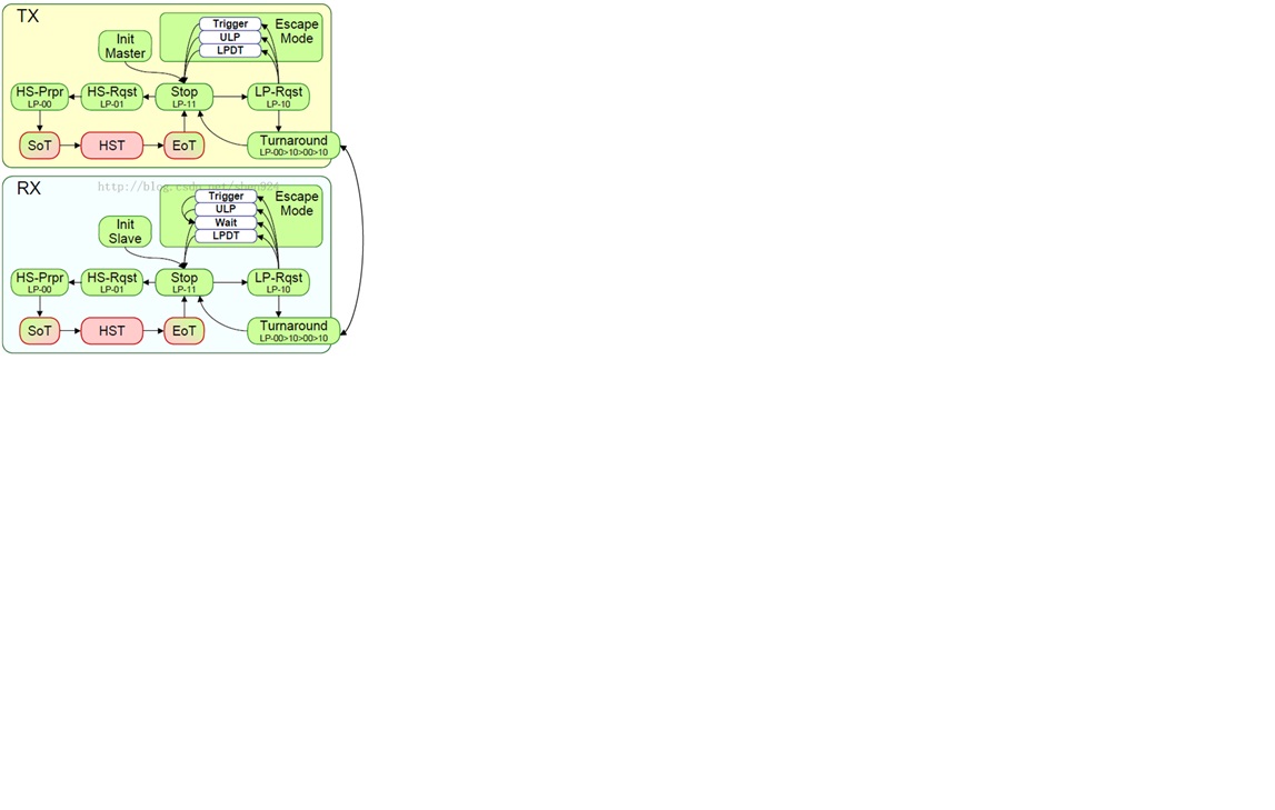
my customer use SN65DSI83-Q1 to convert MIPI to LVDS(LCD display), now it can display with test pattern, but no display with DSI input. the 0xE5 register data is 0x09.

we check the initial sequence,  it can meet Datasheet, and we also check the DSI input clock, it is OK.

our customer use another vendor's IC in the same board, it can display correctly. 

enclose is the waveform, setting and register data.

I want to know which problem will make the error: 0x09, and how to solve it? please provide you suggestion.--Thank you

  • Hello Zhimin,
    PLL_UNLOCK could be set during initial configuration until the PLL locks. If it can be cleared and stays zero then it’s OK. Have you checked if this bit is being set back to 1 after it’s cleared?
    This is a known behavior of the DSI85 that the CLK is output at a random frequency rate until PLL is locked after the PLL_EN is set to 1.
    I will check the customer's configuration for any miskate.
    Regads
  • Please, provide the panel datasheet.

    The PLL_UNLOCK is the CLK issue, but if you are getting test pattern correctly, it may have been set during the initial setup. You have to check if this bit is being set back to 1 after it’s cleared. If you continue detecting the PLL_UNLOCK error, the input CLK has a signal integrity issue. 

    When DSI Clock is used to derive the LVDS pixel clock, this input must remain in the HS mode during the entire video transition.

    The capture does not show that the DSI signal is in LP11. Make sure you have the MIPI inputs driven to LP11 (both P and N pairs of all MIPI DSI differential pairs to single ended high ~1.2V) prior to asserting EN pin. Please, add markups in the scope captures.

    Also, verify that timing configuration provided by the DSI video source (APU) is also correct per the recommendation generated by the DSI Tuner tool (output tab).

    Video input timing, register configuration and the panel timing requirements all have to match up for video streaming to work without errors.

    The DSI8x does not realign timing. The line time (horizontal sync to the next horizontal sync timing from the APU) on the input is preserved when outputting onto the LVDS interface.  If the line time is different from what is calculated by the tool, this will cause issues.  Even if the DSI source is outputting streams in a burst manner, it is important for the DSI source to fill in the rest of the line time with blanking packets (or LP11) to meet the line time requirement.

    Regards

  • Dear Joel

    Thank you, I ask customer check as your advise, below is the reply:

    1. they clear 0xE5 bit0, IC will set it back to 1. DSI is setting in HS mode when transfer data.

    2. in the wave form, the red one is Enable signal, the yellow is one of DSI data line vs GND. there are 2 reset signal, the first one is reboot, the 2nd reset is created by initial code, when 2nd reset, the DSI data line is set to 1.2V. so I think this is no problem.

     1780.SPEC_CLAA102NDA1CW_V0.0.pdf

    3. for line time, I ask them test the Sync to sync time, they will provide to me later, as I calculate, the time should be 1200pixel/45MHz=2.67us, Is it correct?

    for the 1st issue, how to measure the signal integrity issue? do you mean to use scope to test the distort of the clock/Data, or we have another way to test it?

    enclose is the panel datasheet.

  • Could you please also confirm if the DSI Clock input is driven to LP11 prior to asserting EN pin?

    Check if the PLL_UNLOCK  bit is being set back to 1 after it’s cleared in both modes normal and internal pattern. 

    Could you confirm if the LVDS CLK output running correctly? Correct levels, frequency, no jitter?

    The Output window tab gets activated once all input parameters have been filled in both DSI and Panel Inputs window and the calculator icon is clicked:

    It looks that the DSI Tuner has some problems to show this button in your system. Please, send an email to joel.jimenez@.ti.com,  and I will share a new version. 

    https://e2e.ti.com/cfs-file/__key/communityserver-discussions-components-files/138/2438.DSI83_5F00_config.dsi

    Based on the attached device configuration the line time requirement will be as follow:

    Regards

  • Dear Joel

    Do you mean CLK will drive to LP11 before EN assert(both CLKP and CLKN are set to 1.2V)? I think it is not. below is the waveform, yellow is CLK, Blue is data, green is the EN, another is the DSI clk seems small, is it correct?

    for normal and test pattern, they find both are PLL_unlock.

    line time(Sync to sync time) is 26.667us, meet our requirement.

  • It is required by the MIPI spec for the host to drive DSI outputs (DATA  and CLOCK ) to LP11 prior to the transition to the HS mode. The initialization/transition sequence requirement is per the MIPI DPHY (Section 6.11) and DSI (Section 5.7) spec requirements.

    If DSI interface is driven to illegal states/protocol by the host, the DSI85 may get into undesirable states:
    1. DSI clock or data termination enable may get "stuck"
    2. DSI clock does not get enabled internally correctly

    Unexpected behavior may occur when the EN is asserted(transition from 0 to 1) while DSI CLK  is not in LP11.

    Regards

  • Dear Joel,

    I go to customer side to check this issue today, now they set DSI CLK and Data in LP11 before EN assert, and after send the CSR data that set the DSI to HS mode. but the problem still happen, the 0xE5 data is still 0x09. below is the waveform, the upper one is EN, mid is DSI_CLK, bottom is DSI_Data. in Seq3, they delay 3ms, and seq7 delay 10ms. I think the initial sequence is no problem, Is it OK?

    I also check the line time(Sync to Sync), the time is around 26.67us, meet our requirement.

    and the DSI clk signal is also very clear, no jet.

    I also check the HW, the host SOC is Qualcomm MSM8937, I check the DSI interface between the Host SOC and DSI83Q, check the Voltage, all are correct, and also test 2 boards with DSI clock and reference 27MHz clock, all the Error code are the same(0x09).

    now I do not have any idea how to make it work. Do you have idea how to solve the problem?--Thank you.

  • Hello, 

    Before or when video first starts, DSI_CLK p/n should transition from LP state to HS (high speed - differential signaling) state following the DSI/DPHY protocol.Then DSI_CLK runs continuously and should never go back to the LP state (1.2v). As stated in the datasheet:

    When the MIPI D-PHY channel A HS clock is used as the LVDS clock source, the D-PHY clock lane must operate in HS free-running (continuous) mode.

    Regards

  • Dear Joel

    we follow this issue, we set DSI CLK from LP11 to HS prior then output the video stream, you can find it in above the waveform(yellow is CLK, blue is Data), the differential signal of CLK start before Data start. 

    in the software, the DSI host keep in HS mode in all transmit of the data, and we also try to use the DSI clk as LVDS clock and use external clock source(27MHz reference clock) as LVDS clock. but the problem are the same.

    so I do not know whether there is any other wrong will cause the problem. Do you have any other advise(for example reduce the DSI clock or DSI refresh rate)?

  • Hello Zhimin, 

    In the scope capture above, the DSI clock signal (blue) goes from HS to LP mode, that is why I mentioned that per requirement the DSI clock should be HS continuous. Having LP state in the DSI Clock, when it is used as a clock source, can cause issues with the PLL.

    For the external 27MHz clock case, as per your configuration, the output LVDS clock will be 54Mhz, which is not supported by the panel since the max Clk frequency is 50Mhz. You will need to change to either a 25Mhz or a 45Mhz external clock. 

    For the case when the DSI clock is the clock source, check if the LVDS CLK output running correctly. Correct levels,  frequency (45MHz), no jitter. Also, confirm that the DSI clock is running at 135Mhz.  Could you try using a 270 MHz DSI clock and a divisor of 6. 

    Try adjusting the CHA_LVDS_VOD_SWING. Perhaps try changing this to default (11) or next step up (10).

    Regards

  • Dear Joel

    thank you for your help

    the blue signal is DSI data, the yellow signal in middle is DSI clk. so I think in EN assert, the DSI data and CLK are in LP11, after around 50ms delay, the DSI CLK turn to HS mode(there is continue signal of yellow signal in the mid), you can find there is some command in blue and after some time, there is data signal on blue.

    for second, I have told customer, the main effect is there are some noise on the panel in test pattern, they said they can change the frequency later.

    for the third,  I suggest customer reduce the refresh rate from 60Hz to 48Hz, they will test today. I think this will be better, because if we increase the frequency, there will be more EMI and the time requirement will be more critical. Is it OK?

    for the fourth, I can not understand, it seems the register is adjust the Vod of output LVDS, does it effect the receive of DSI signal?

    I also search the MIPI specification from website, I find between LP11 and SoT, there are 2 stages(LP01 and LP00), Do we need insert the 2 stages before output video stream from host? I will also ask customer check this to Qualcomm.


  • Hello zhimin,

    Ok, the initialization sequence looks correct. Just confirm that the CSR registers are initialized before starting the DSI video stream.

    A few things you can try:
    - If DSI input is being affected by the EMI/noise, try to adjust the EQ value at addr 0x11. Default is 0x00 with no equalization, try 01b or 11b and see if the issue improves on both DSI_DATA and DSI_CLK
    - If there's noise issue on LVDS output/panel input, the LVDS_VOD swing can also be adjusted at addr 0x19.

    If these errors are occurring all the time, then you need to check timing on DSIA interface (setup/hold).  Maybe you can change DSI86 RXEQ level (register 0x11) to see if errors go away.

    Regards

  • Dear Joel

    Thank you. 

    I am sorry, I do not tell you I have set the EQ to test before, but it do not have effect.

    yesterday, I was on trip and do not have time to ask customer's test result. I will check today, and if there is any feedback, I will tell you.--Thank you.

  • Dear Joel

    customer change the refresh rate to 48Hz, but no improve.

    TI Shanghai FAE Alpha Han hope to contact with local Qualcomm engineer to check whether there is any conflict between DSI83Q and MSM8937. if you know any Qualcomm engineer, can you also help check this issue with them?

    I am very appreciate your support in the case.--Thank you