This thread has been locked.
If you have a related question, please click the "Ask a related question" button in the top right corner. The newly created question will be automatically linked to this question.
Hi Team,
My customer is facing the issue that FPGA is stuck sometime when issuing Data path reset on TLK10232. As far as we check the FPGA error status, it seems that FPGA gets Alignment error at XAUI line at the timing and can not sync again due to some reason.
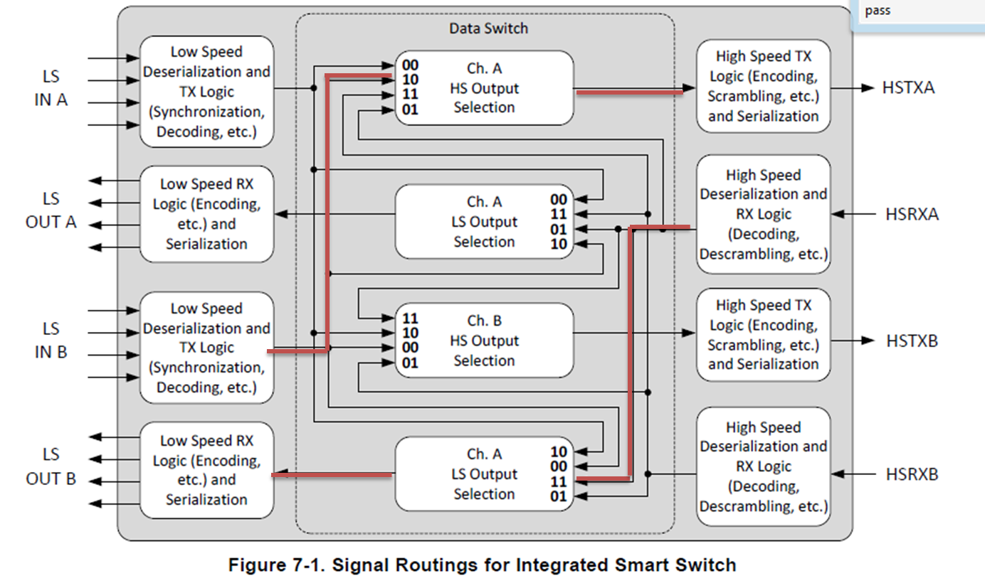
According to datasheet, TLK10232 automatically converts /A/, /K/ and /R/ character to Idle and outputs "Idle" pattern only(between data packet) on XAUI line continuously as default. We are guessing that this might be root cause of this issue.
Are there any registers to issue the characters for XAUI lane alignment?
The customer is using TLK10232 in 10G KR mode, so FORCE_LM_REALIGN register change doesn't work because this register is only for 10G-KX mode.
(I think that PCS_RX_DEC_CTRL_CHAR may be used, so please let me know if you know how this register behaves. )
Regards,
Takashi Onawa
What is the value of these registers:
DST_CONTROL_1
DST_CONTROL_2
DSR_CONTROL_1
DSR_CONTROL_2
DATA_SWITCH_STATUS
As well, what is the value of DST_PIN_SW_EN pin?
I am asking this because it seems a data switch issue.
Thanks,
Luis
Hi Luis-san,
DST_PIN_SW_EN pin is not used.
Here is the values which you requested.
- ChA
Switch control registers
Changed only DST_CONTROL_1 as below
DA:0x1E RA:0x0017 WriteData:0x2014
Other SW settings as same as default
DATA_SWITCH_STATUS
The second read value is as following.
4020h
I see DST and DSR ON/OFF bit asserted in first read value after the data path reset.
- ChB
Switch control registers
Changed only DSR_CONTROL_1 as below
DA:0x1E RA:0x0019 WriteData:0x2518
Other SW settings as same as default
DATA_SWITCH_STATUS
The second read value is as following.
1080h
I see DST and DSR ON/OFF bit asserted in first read value after the data path reset.
Regards,
Takashi Onawa
Hi Takashi-san,
According to the block diagram that you sent before, customer desires this data path:
CHA
LSINB ==> HSTXA
CHB
LSOUTB <==HSRXA
Hence, they need to configure the data switch register as follows:
CHA
LSINB ==> HSTXA
DST_CONTROL_1
Write 0x2000
MDIO control, DST_PIN_SW_EN = '0' (Default)
DST_CONTROL_2
Write 0x2C20 (Select alternate channel LS input)
CHB
LSOUTB<==HSRXA
DSR_CONTROL_1
Write 0x2500
MDIO control, DST_PIN_SW_EN = '0' (Default)
DSR_CONTROL_2
Write 0xCC20 (Select alternate channel HS input)
Please implement this configuration and let me know your results through the register DATA_SWITCH_STATUS. By the way, what is the current value of PRTAD0 pin?
Thanks,
Luis