This thread has been locked.
If you have a related question, please click the "Ask a related question" button in the top right corner. The newly created question will be automatically linked to this question.
Hi Team,
would you please help with below question from my customer? thanks.
Customer have questions about DSI CSR settings in DSI tuner at normal mode operation.
the resolution of the panel is 1080*2400,
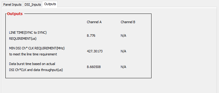
1 port MIPI, hbp=40/hfp=120/hsa=10/vbp=6/vfp=8/vsa=2, MIPI clock= 433MHz
2 port LVDS, hbp=90/hfp=120/hsa=10/vbp=6/vfp=9/vsa=2, LVDS clock = 433MHz/5 = 86.6MHz
would you please suggest how to set the Hactive of port A and port B of LVDS? should it be 540 or 1080?
Customer have tried to set LVDS Hactive = 540, the capture shown as attached, the first 5 lines U_ib_rx_ctrl/lvds_rx_de[3:0] is the DE signal, the width of DE signal is 540 pixel clock.
then, the next signal is HSYNC, customer have measured that hsa=10/hbp=90 which meet the setting. but hfp is much longer than 120 picel clock, also there are 1525 pixel clock between two HSYNC, which indicate the line time is incorrect.
so, would you please suggest how does DSI85 generate HSYNC signal? is it set by CSR? or generate from the MIPI signal?
thanks.
Kevin
Hello Kevin,
We suggest using our DSI Tuner utility to generate the register configuration base on your panel and GPU capabilities. Please, export the .dsi file using the tool since it contains important timing requirements calculated from your settings.
For a dual LVDS configuration the value of the CHA_ACTIVE_LINE_LENGTH will depend on whether you select pattern mode. In normal operation you should program 1080. You can also generate the correct setting for both modes using our DSI Tuner.
What matters most is that the DSI video input is presented per the timing configuration generated by the DSI tuner (output tab). Video input timing, register configuration and the panel timing requirements all have to match up for video streaming to work without errors. I meant DSI video timing needs to meet the line time requirement which is based upon the LVDS panel inputs entered into the tool.
The DSI8X retains the timing of the input to the LVDS output. Therefore, it is important to provide the data at the DSI input per the panel requirement.
The device datasheet motions this requirement:
Figure 18 illustrates the DSI video transmission applied to SN65DSI85 applications. In all applications, the LVDS output rate must be less than or equal to the DSI input rate. The first line of a video frame shall start with a VSS packet, and all other lines start with VSE or HSS. The position of the synchronization packets in time is of utmost importance since this has a direct impact on the visual performance of the display panel; that is, these packets generate the HS and VS (horizontal and vertical sync) signals on the LVDS interface after the delay programmed into CHA_SYNC_DELAY_LOW/HIGH (CSR 0x28.7:0 and 0x29.3:0) and/or CHB_SYNC_DELAY_LOW/HIGH (CSR 0x2A.7:0 and 0x2B.3:0).
Regards
The .dsi file is attached.
Please kindly advise if it is correct or not. Thx.
/cfs-file/__key/communityserver-discussions-components-files/138/0606.7z