This thread has been locked.

If you have a related question, please click the "Ask a related question" button in the top right corner. The newly created question will be automatically linked to this question.

p82b96: Can P82B96 be used for the attached connection diagram?

Part Number: P82B96

 Hello guys,

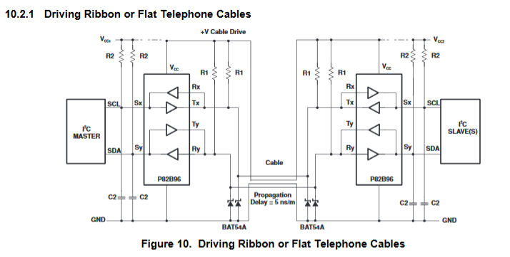
 One of our customers wants to use P82B96 with the connection as the attached PDF file to control a few I2C devices on a few PCB boards with a few meters.

 Could you please take a look the attached file and could you please give me your reply whether the connection in the file is promlem or not?

 If the connection is wrong, could you please tell me the correct connection?

 Your reply would be much appreciated.

 Best regards,

 Kazuya Nakai.p82b96_connection(NakaiMod031418).pdf    .

  • Hey Kazuya-San,

    "Could you please take a look the attached file and could you please give me your reply whether the connection in the file is promlem or not?"

    -I do see a potential problem with this set up. The P82B96 is like many of our other I2C buffers in the sense that it uses static voltage offset. The issue here is I/Os with static voltage offsets cannot be connected to each other because the static voltage offset may not pass a low to another device with a static voltage offset (offset side to offset side connected to each other) in certain conditions. Below you can see this recommendation discussing this in the datasheet:

    " If the connection is wrong, could you please tell me the correct connection?"

    What I would recommend is connecting the device not at the Sy/Sx points but on the T/R I/Os.

    Some things I would watch out for:

    1. This device supports up to 4000pF, in the configuration I suggested above you will be stacking the capacitance up with each wire/harness you connect so you need to keep in mind the 4000pF limit.

    2. Pull up resistors may need to be sized up or down depending on how many boards are connected. Each pull up resistor on the P82B96 T/R lines will be stacked in parallel with each other. If you stack a bunch of pull up resistors in parallel, you could damage our device (minimum current sink ability is 60mA though typical is 100mA but varies with temperature).

    3. With longer wires, you may start to see the effects of inductance (parasitic) which can cause inductive kickback events to occur. This can damage our device when a signal is high but then pulled low, the ringing on the low could reach very high negative values and damage the device. Maximum for our device looks to be -0.3V. To ensure this does not happen, you should place schottky diodes on the T/R lines. You can see an example of this below with the BAT54A devices below:

    Lastly, may I ask what application or end equipment you are using this device for? I am always interested in hearing where customers use this device. 

    Thanks,

    -Bobby

  • Hello Bobby,

    Thank you very much for the prompt reply.

    Your reply is helpful for the customer and me!

    Thank you again and best regards,
    Kazuya Nakai.