This thread has been locked.

If you have a related question, please click the "Ask a related question" button in the top right corner. The newly created question will be automatically linked to this question.

DP83848C: Schematic review, odd waveforms, FCS errors, and request for a few debug ideas

Part Number: DP83848C

Hi, I just started working today on a problematic board previously designed, but it's high priority and I need to attack from several angles. Issues with intermittent FCS errors on TX and so far only noted in the switch. Working on more data.

First, if someone could please take a quick look at the schematic, that would be great (below).

Known issues/concerns:

  • The top of C519 and C520 should have been connected, correct?
  • Any idea why are R517 and R518 are not 49.9 ohm. Bizarre. Any theories? Regardless, I will change. Just curious if they are ever not 49.9 for any reason, such as signals not routed as 100 ohm differential.
  • Datasheet calls out 10uF PFBOUT cap as tantalum, and we have a ceramic capacitor with much lower ESR than perhaps intended. Do you have a recommended specification here? Will X5R MLCC not work better? What is the PFBIN rail for?
  • Not shown in schematic, but we have the same 50MHz reference clock feeding both the reference here on pin 34, and the RMII interface on a STM32F MCU, without a fanout buffer, and poorly routed. For future circuit improvement, do those two reference clocks have to be aligned, or could they be separate 50MHz oscillators with 50ppm or better?

I hope to post for some help tomorrow on layout concerns, and start the process of some loopback tests from a traffic generator.

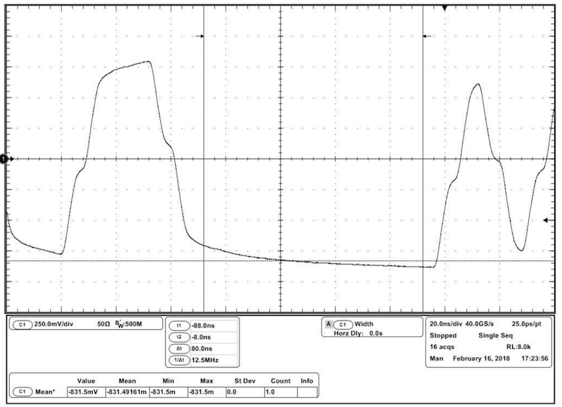
One other initial oddity: a test engineer did some work with a differential probe on the signals.

TDP3500 - Differential probe,
TDSET3 – Ethernet compliance test automation software

Transmit waveform on TX lines looks like this

:While transmit on the RX lines looks like this:

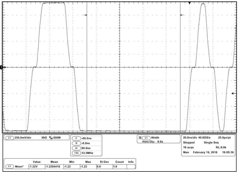
Any ideas for the poor shape? Is the center hitch from reflection? Sorry, I don't know where probe was placed. The first image also looks perhaps like poor length matching?

Thank you.

5756.Ethernet.pdf

  • Any updates? Schematic feedback?

    Thanks!

  • Hi Gary,

    Your comments above are correct.
    Please replace the 82 ohm resistors with 49.9 ohm resistors.
    When doing TX and RX testing, are you using a 100 ohm termination and probing across the termination?

    Yes, please use a tantalum capacitor. We need the ESR for our internal regulator.

    The rest of the schematic looks good.

    When probing the MDI and looking at the waveform are you forcing MDI and MDIX operation to be able to see the waveform on both TD and RD pins?
  • Do you have a target ESR for the capacitor? Circuit today only has an 0603 spot, and the tantalum's that fit are not polar and relatively low ESR (for tantalum). But, we are spinning the board asap.

    Thank you.

  • Also, do the reference clocks feeding both the reference here on pin 34, and the RMII interface on a STM32F MCU have to be aligned (synchronized, same source), or could they be separate 50MHz oscillators with 50ppm or better?

    And what is the PFBIN rail for?

    Thank you again.
  • Any update on ESR recommendation, clock synchronization requirement between PHY/MCU interface (I think it unlikely requirement), and some insight into what PFBIN is for? The 10uF Tantalum is not specifically defined in the BOM and is just generic; huge variability in available options with ESR. Looking for a few pointers on these things so we can complete our spin of the board.

    Thanks.
  • Hi Gary,

    The ESR should be a few ohms. The 50MHz clock on XI must be synchronized with the clock fed to the MAC. When in RMII operation there is no dedicated clock pin like there is for MII. In MII you have TX_CLK and RX_CLK. For RMII, the reference clock into the PHY at XI serves as both RX_CLK and TX_CLK.