Part Number: P82B96
Other Parts Discussed in Thread: HDC1010,
Hello there,
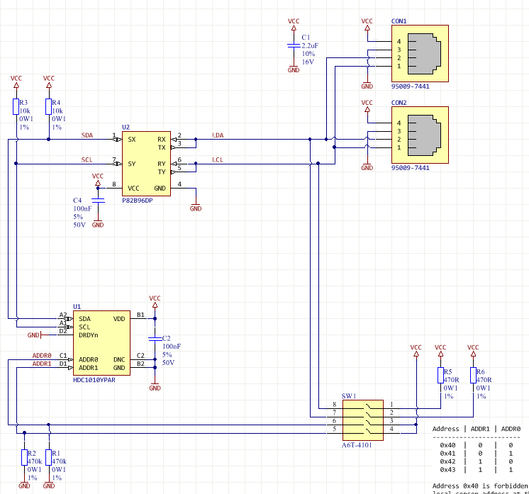
I am working with a system that can be expressed in such block diagram:

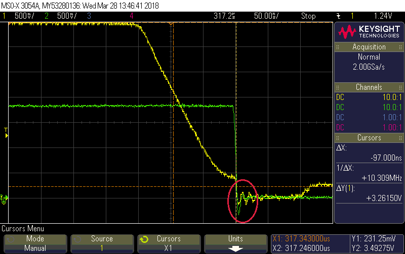
My problem is the following: At the start of the program i check each device (7 bit addresses from 1 to 127) for presence (wait for ACK). The HDC1010 connected on the other side of extended network is acknowledging, but then something happens to the bus and the SDA line is not properly pulled up anymore. Its like the net is in some kind of deadlock (0x41 address). I suspect this to be the cause of the P82B96's, as this doesnt happen if I connect HDC1010 directly to the MCU I2C bus. Here are the scope views:
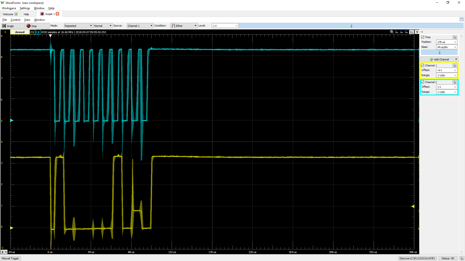
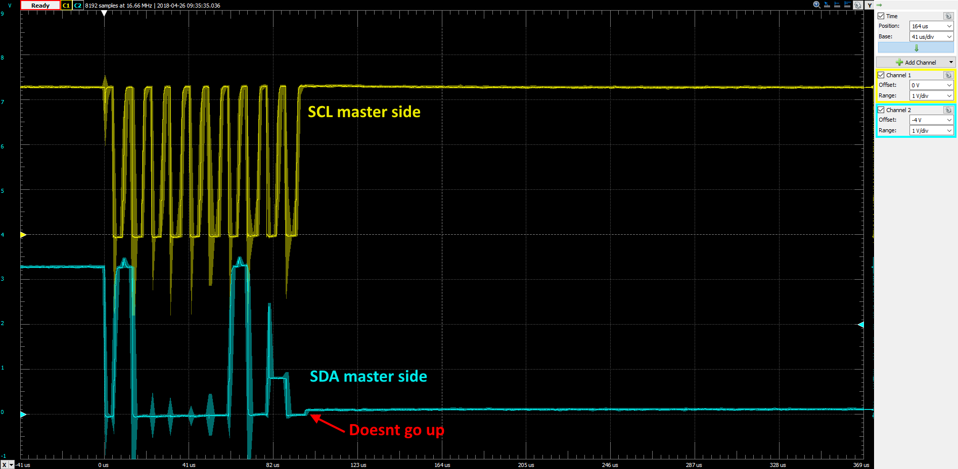
Master side:
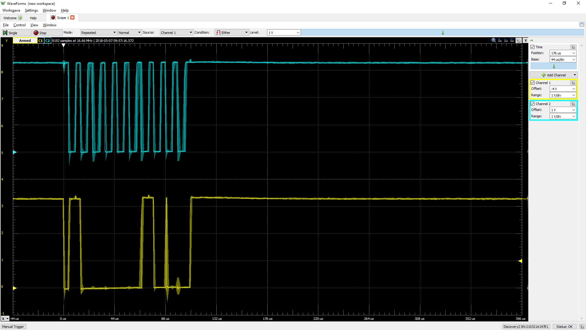
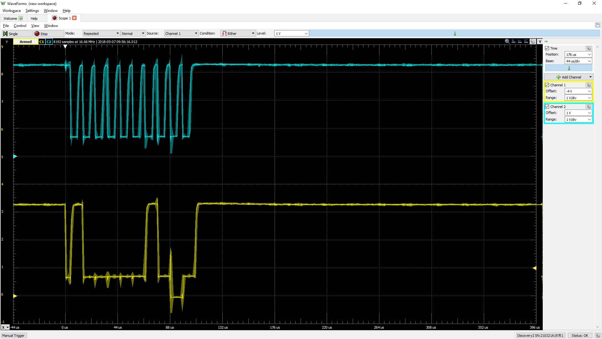
Slave side:
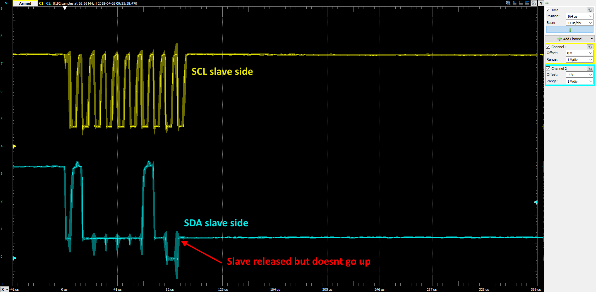
The low level "read" by a device is not exactly 0V but around 0.7 V, but thats understandable since I2C buffers are used. The problem is that after the ACK the SDA line should go up, but it doesnt. I am struggling with this for a while now and out of ideas. Also let me say that this problem did not occur from the beggining, but only after couple days and persists now. I checked all pull-up resistors and they are ok. I would really appreciate all help as the case is urgent for me.