Part Number: DS90UB948-Q1
Hello,TI Experts,
I have below questions about DS90UB948 need your help:
1.What's the meaning of T1 and T2 in Power sequence~
Is it T1 for VDDIO delay time ,T2 for VDD12 delay time ?
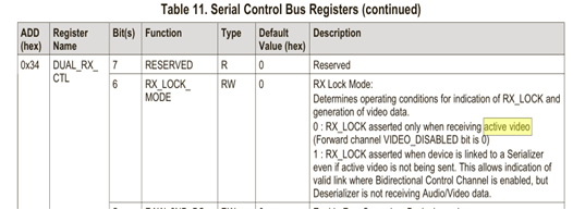
2.How to understand active vedio?If the resolution is wrong, will there be a lock signal?
figure 2
3.Is their pattern inside DS90UB948,when their is no LVDS input signal,Will it output the default image?
4.How does CDC host reset DS90UB948 by HSD ? is it by PDB pin? How to make it?
5.Can I use only one LDO for both VDDIO and VDD33, use Bead to isolate them?
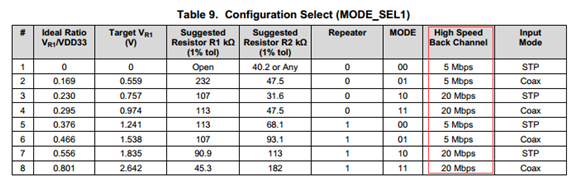
6.Their is High Speed back channel in MODE_SEL1, Does it mean the FPDLINK's transmission rate?
figure 3
7.What's the meaning of PIN1(Lock)? What should the MCU feedback to the output signal?
8. Is PIN4(BISTC) a channel of CLOCK signal?MCU must provide a channel of reference clock,then it can self test?
Looking foward to your raply,thank you very much~