


Part Number: DP83867CS
Hi,
The DP83867CS PHY will be used as a normal SGMII interface. The VDDIOx supply is powered with 2.5Volt.
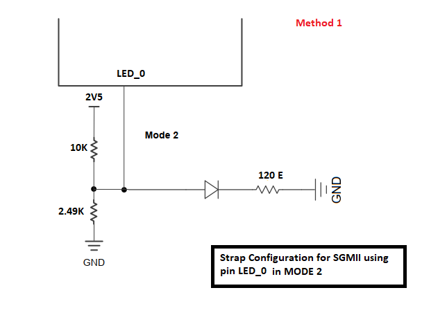
The datasheet suggests that while strap configuration, LED-0 has to be kept in MODE-2 to enable PHY in SGMII mode during power up.
Q1. Which is the recommended schematics for connecting LED-0, Method1 or Method2? Kindly sugesst.

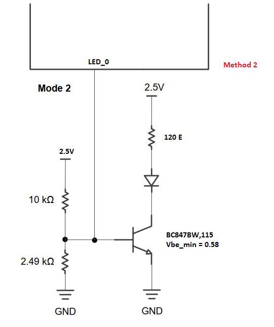
Q2. If Method2 is chosen is there any specific requirement to be followed while selecting the transistor, like 'Vbe of transistor should be greater than 0.191 x VDDIO (= 0.4775V)' etc..?
Q3. The Transmit, Receive and Clock lines in SGMII mode is having AC copling capcitor. In PCB layout, during placement which is the preffered position to keep these capcitors? Is it nearer to 'PHY' or or is it nearer to the 'FPGA(MAC)'?
Regards
DEEPAK V