This thread has been locked.

If you have a related question, please click the "Ask a related question" button in the top right corner. The newly created question will be automatically linked to this question.

XIO3130: Clock is not Generated in Down Stream Port

Part Number: XIO3130

Hi,

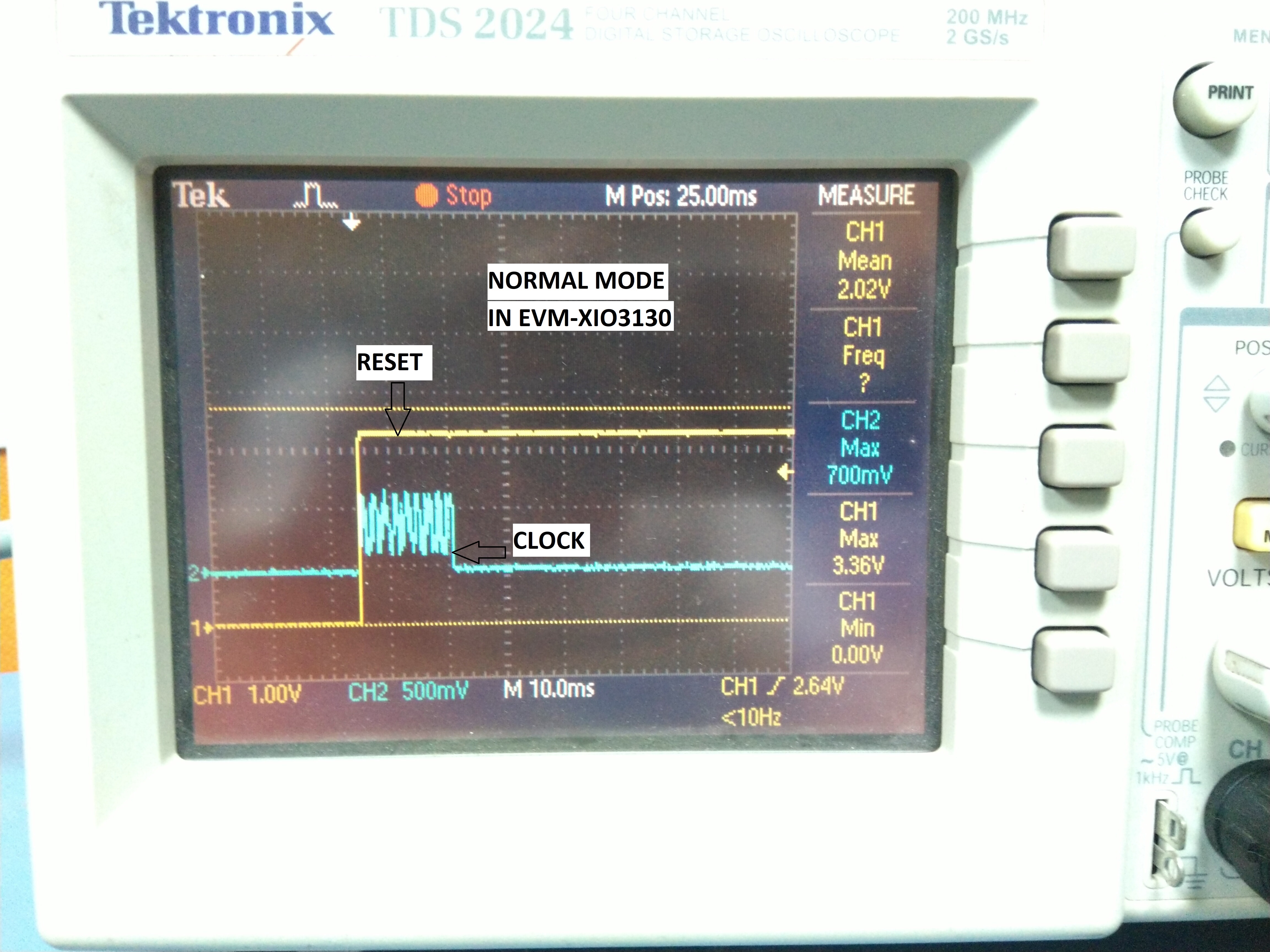
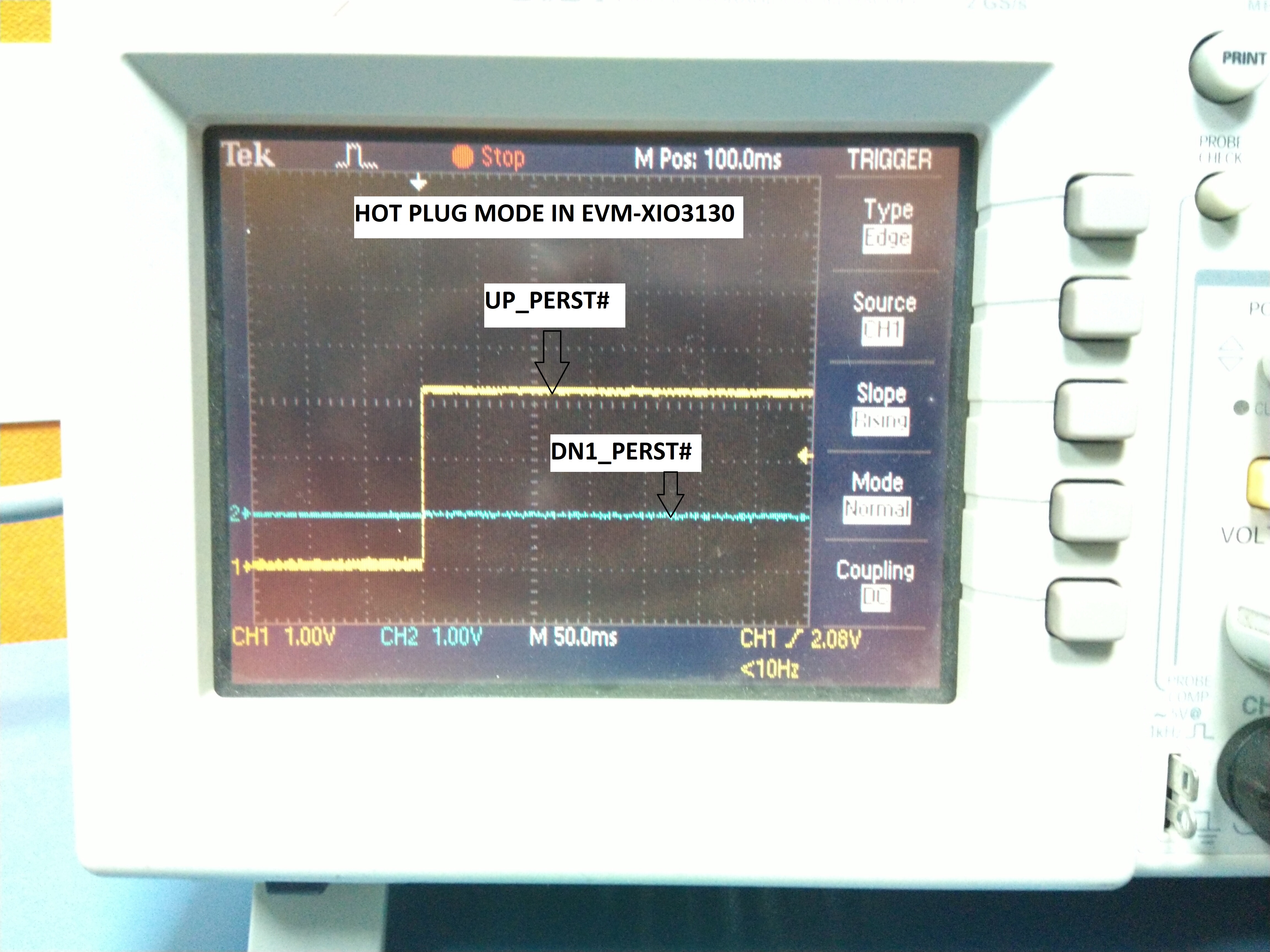
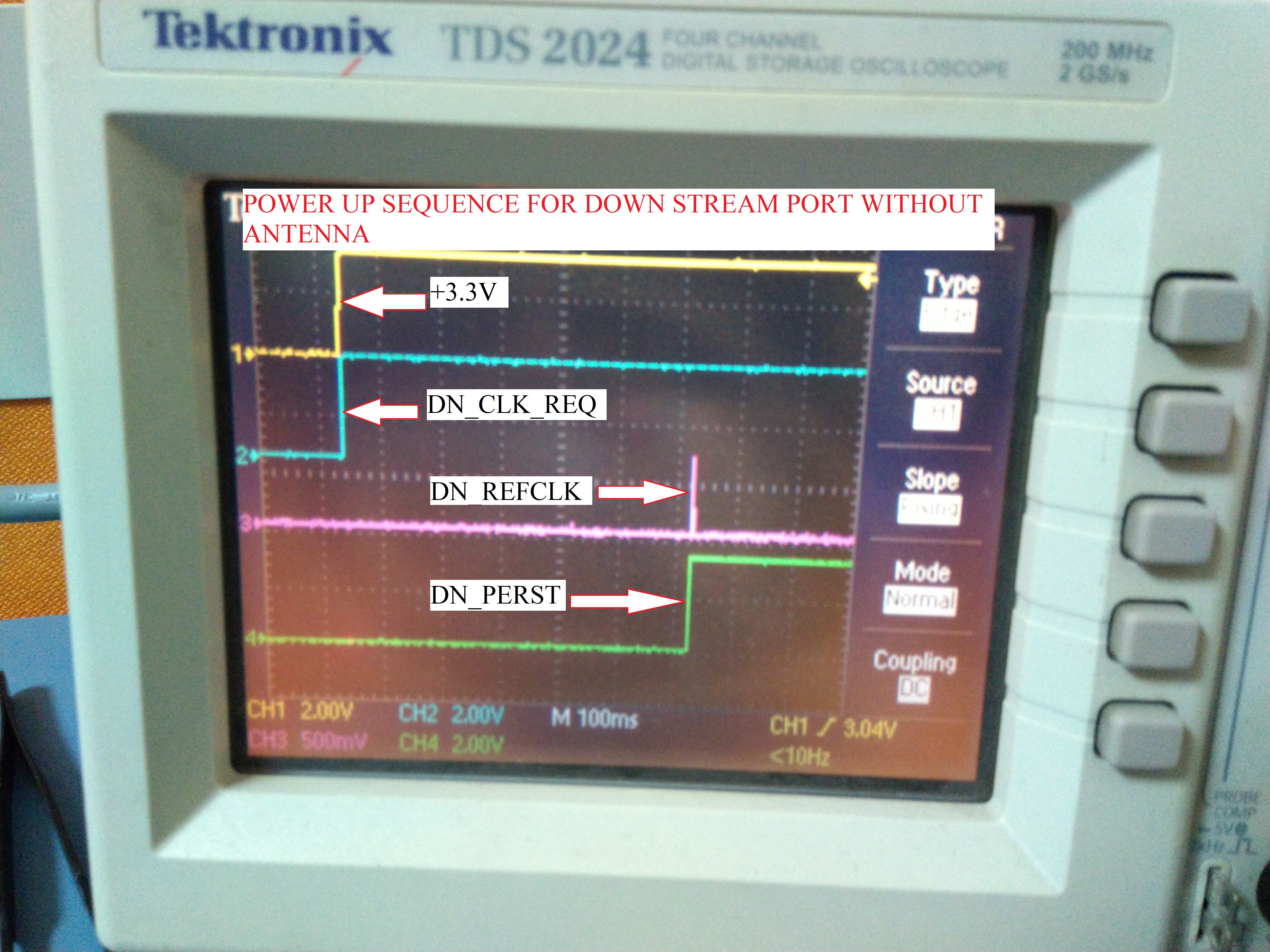
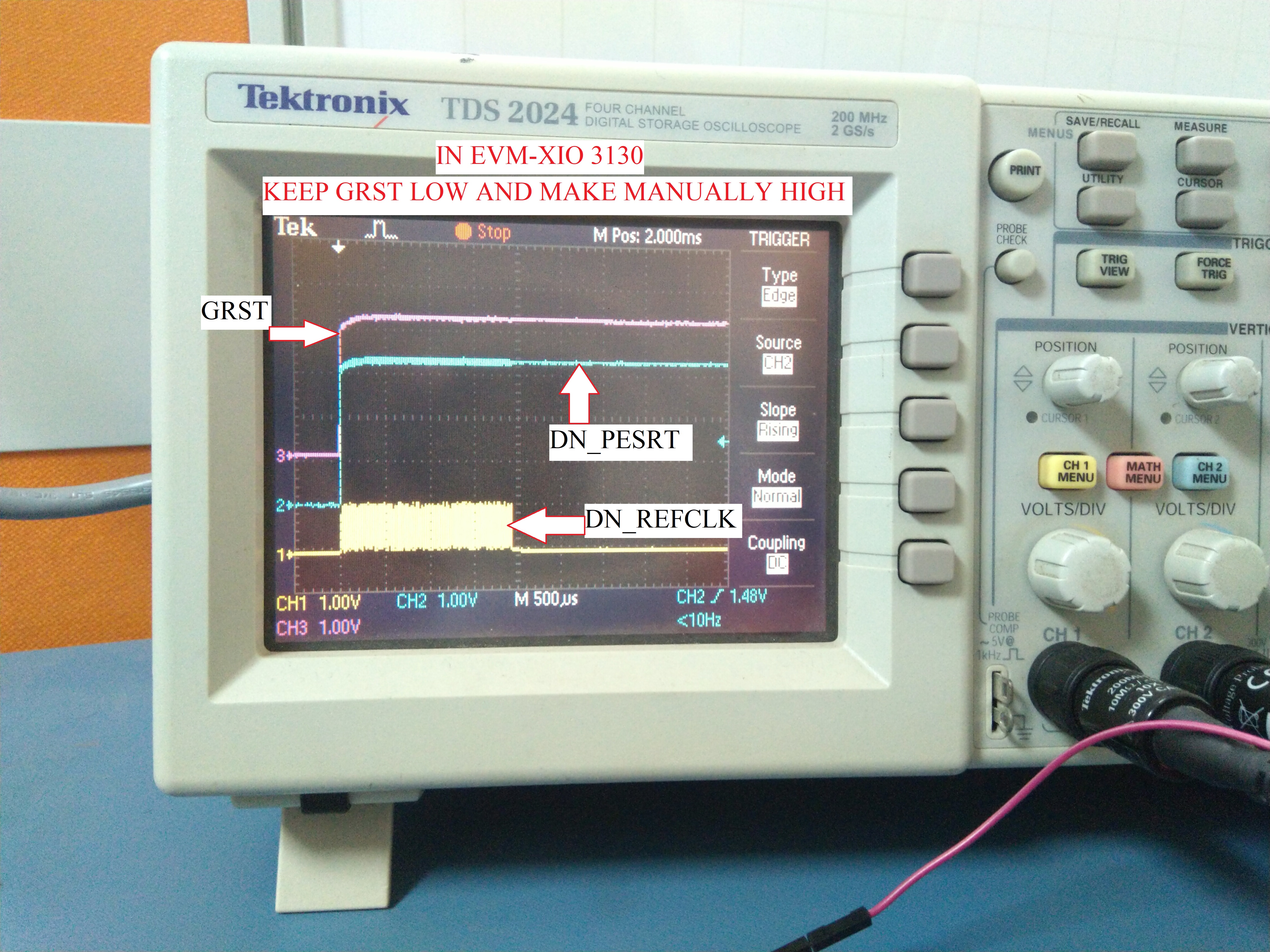
I am using XIO3130 in current design. 

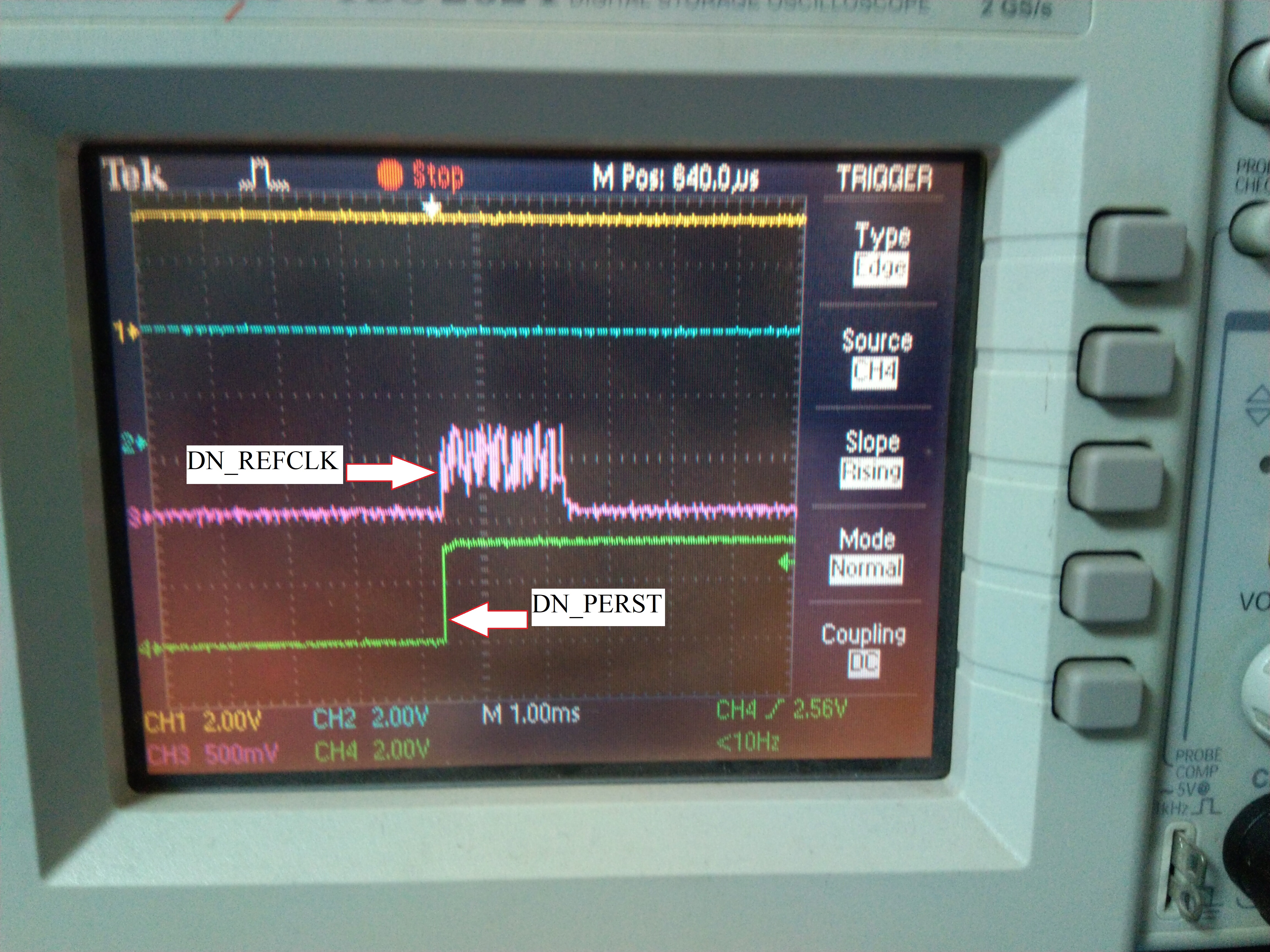
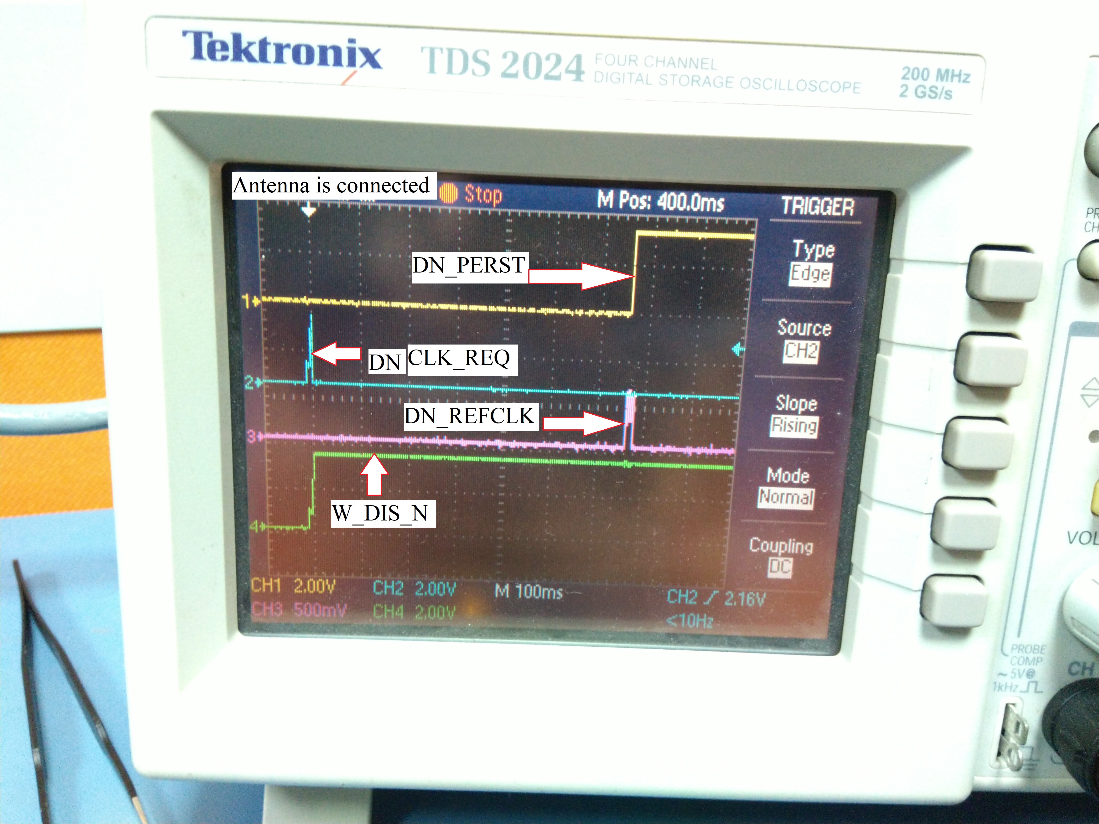
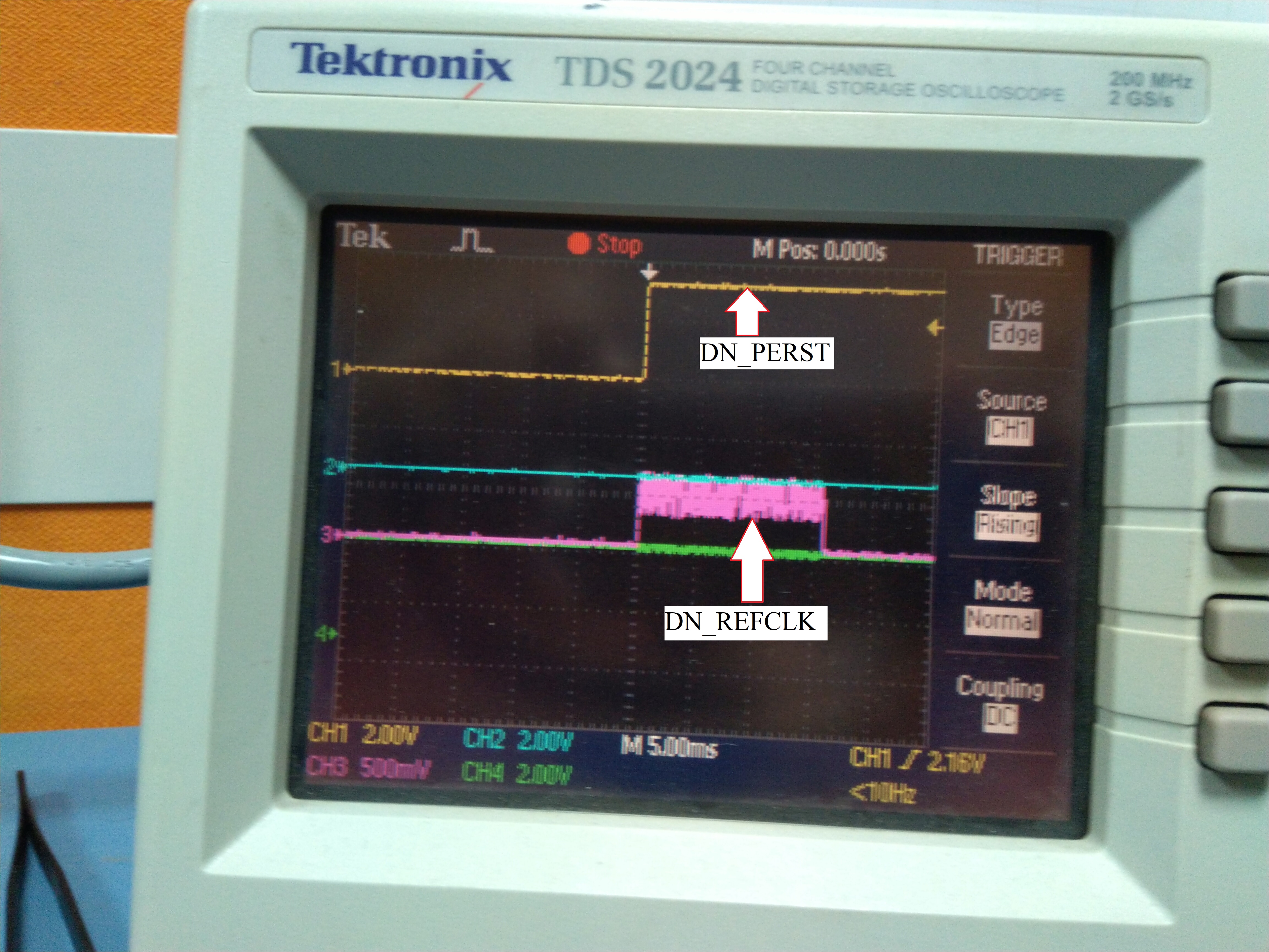
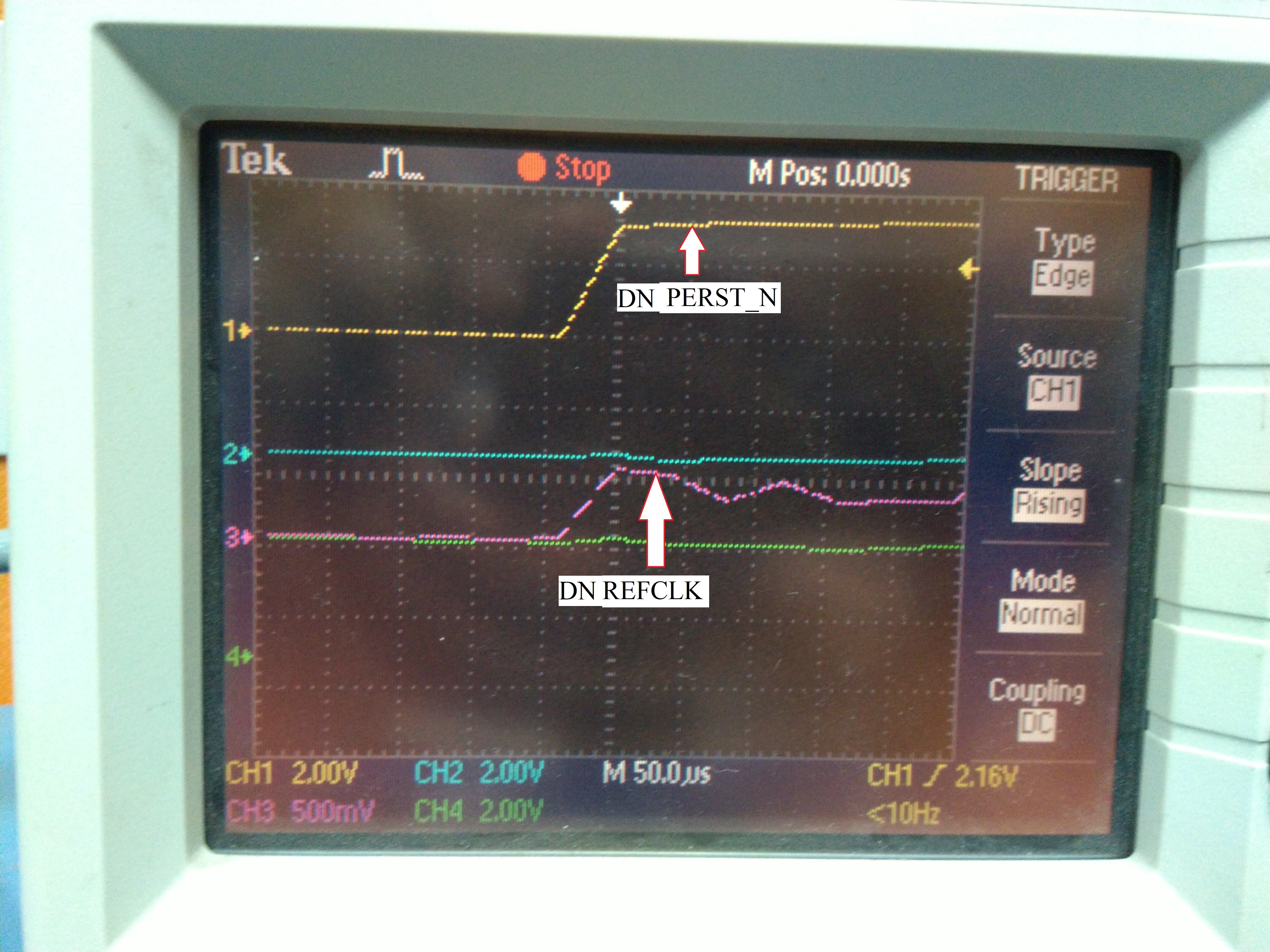
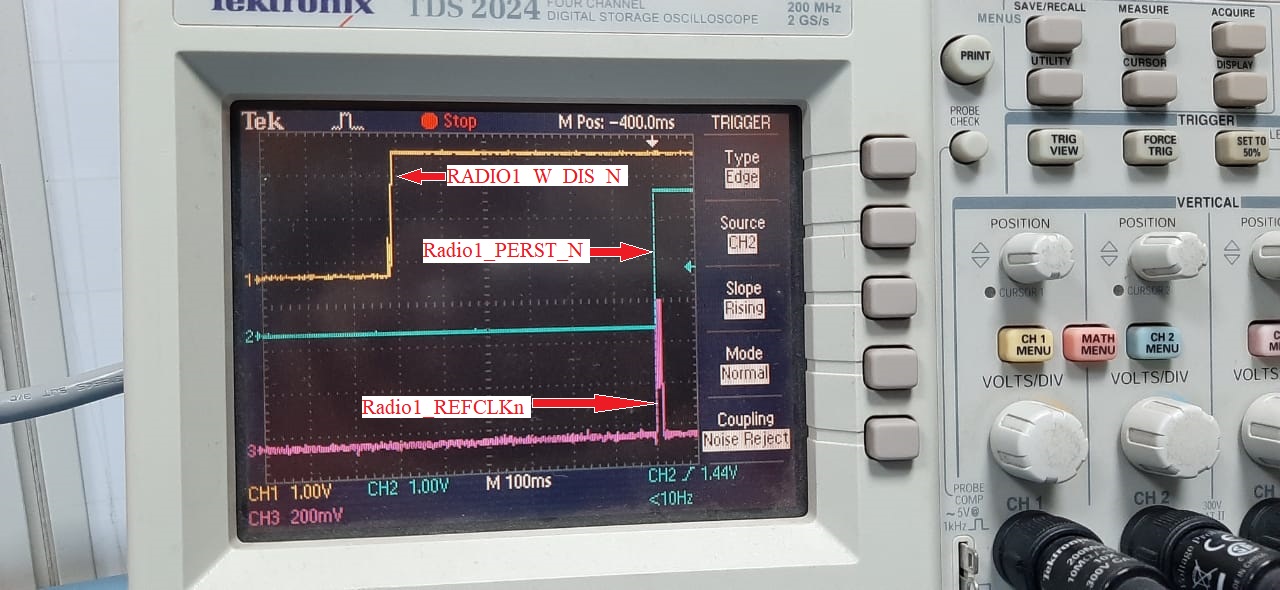
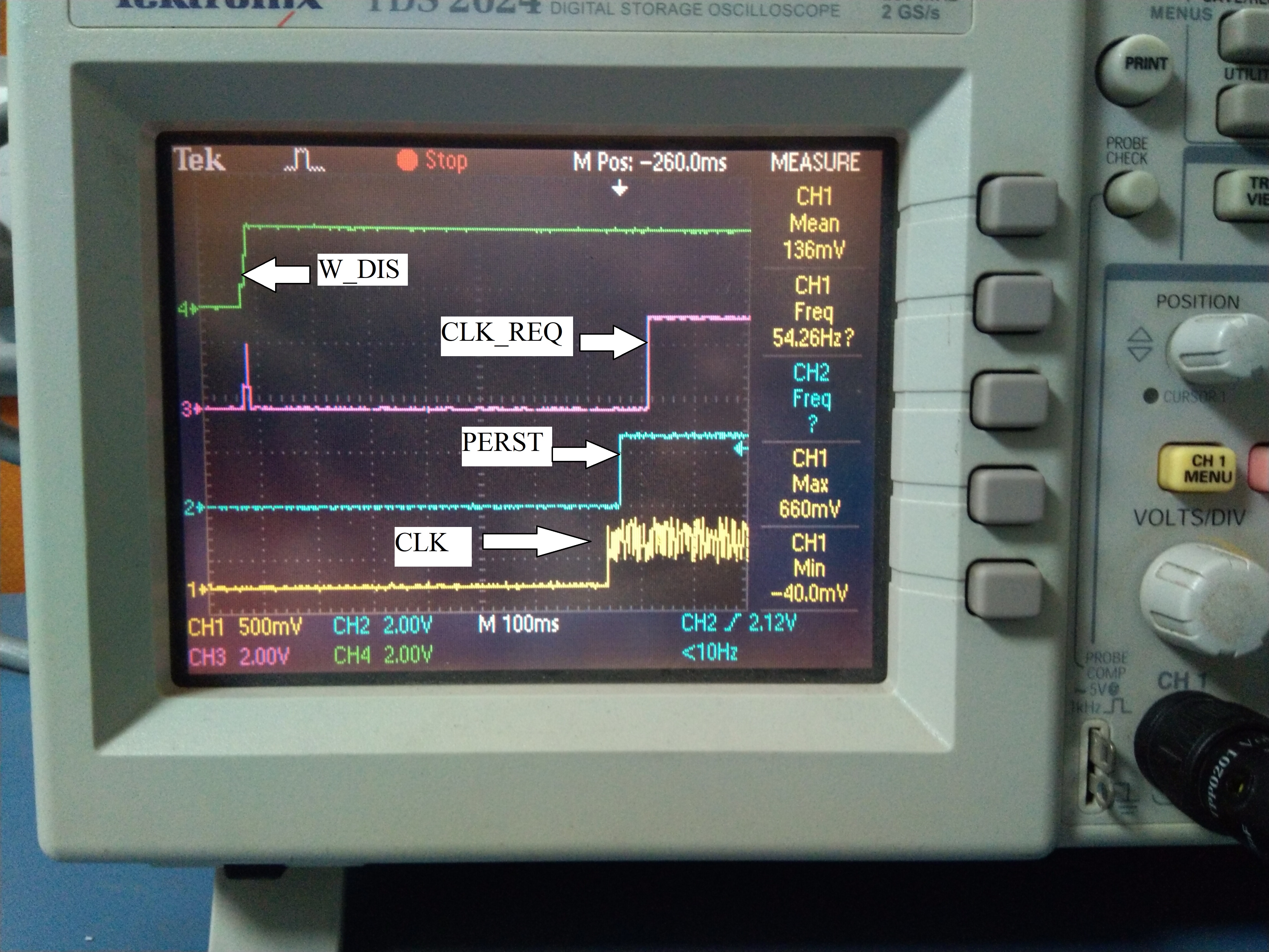
We have connected Third Party Antenna Board on all three Downstream Port.

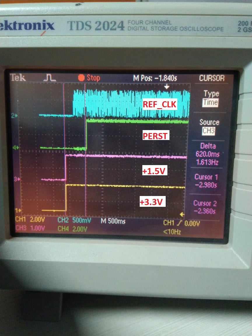
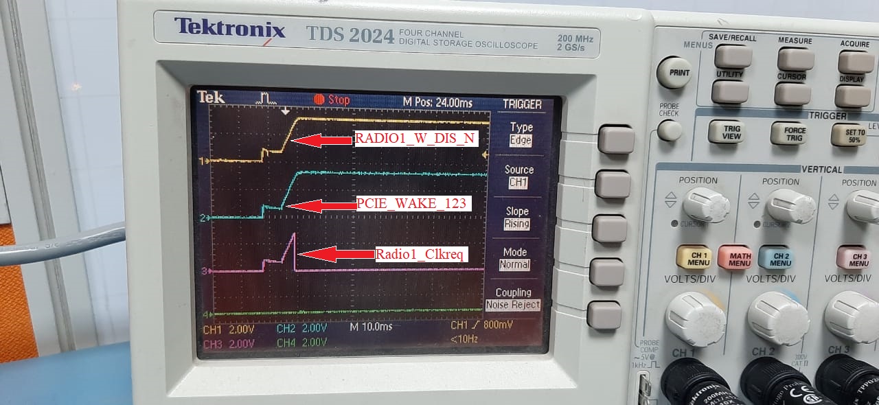
Below is the signal behavior between XIO3130 and Antenna Board.

Also find the EEPROM file configuration which we are using for testing.

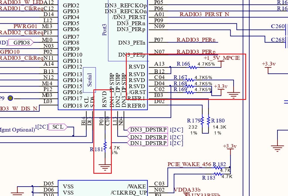
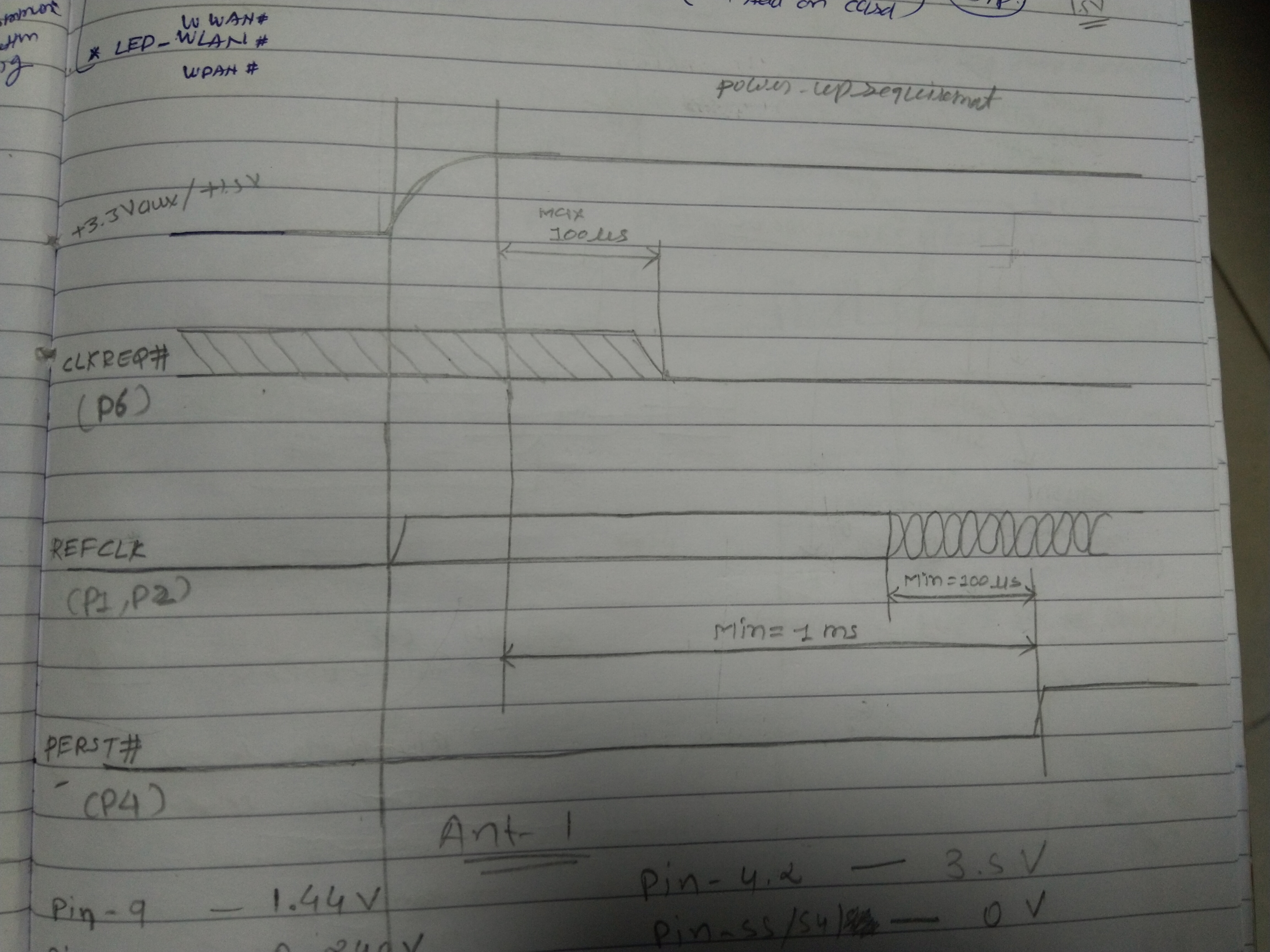
How should the Downstream port clock will be generated from XIO3130?

Should we need to set the configuration in EEPROM?

Kindly provide your valuable input.

Regards,

Alpesh.

000	4C	01000111
001	00	00000000
002	24	00100100
003	00	00000000
004	04	00000100
005	00	00000000
006	00	00000000
007	00	00000000
008	49	01001001
009	00	00000000
00A	89	10001001
00B	10	00010000
00C	50	01010000
00D	12	00010010
00E	49	01001001
00F	01	00000001
010	27	00100111
011	F2	11110010
012	07	00000111
013	00	00000000
014	01	00000001
015	00	00000000
016	00	00000000
017	00	00000000
018	00	00000000
019	14	00010100
01A	32	00110010
01B	02	00000010
01C	00	00000000
01D	00	00000000
01E	00	00000000
01F	00	00000000
020	00	00000000
021	00	00000000
022	00	00000000
023	00	00000000
024	00	00000000
025	24	00100100
026	3F	00111111
027	04	00000100
028	01	00000001
029	00	00000000
02A	01	00000001
02B	00	00000000
02C	00	00000000
02D	00	00000000
02E	00	00000000
02F	14	00010100
030	32	00110010
031	12	00010010
032	00	00000000
033	1A	00011010
034	00	00000000
035	00	00000000
036	02	00000010
037	00	00000000
038	01	00000001
039	00	00000000
03A	00	00000000
03B	00	00000000
03C	00	00000000
03D	14	00010100
03E	32	00110010
03F	12	00010010
040	00	00000000
041	1A	00011010
042	00	00000000
043	00	00000000
044	02	00000010
045	00	00000000
046	01	00000001
047	00	00000000
048	00	00000000
049	00	00000000
04A	00	00000000
04B	14	00010100
04C	32	00110010
04D	12	00010010
04E	00	00000000
04F	1A	00011010
050	00	00000000
051	00	00000000

  • Hello,

    We will look into this and get back to you.  Have you looked at the errata below?  There is an item related to downstream reference clock.

    Regards,

    Yaser

  • Hi Alpesh,

    Are you still having issues? Did the workaround in the errata help any (ie operating the device in hot plug mode)?

    Regards,

    I.K. 

  • Hello I.K.,

    Thanks for your reply.

    Workaround in the errata did not help us as it is not relevant to our issue.

    As per our application, we are using EEPROM in Normal mode (You can also refer the schematic which was share with you earlier).

    The problem was described on first thread and still not resolved.

    Kindly check from your side and suggest your valuable feedback.

    Regards,

    Alpesh.

  • Your device is operating in normal mode so it may be related to the problem in the errata. Have you tried the workaround?

    Regards,

    I.K. 

  • Hello I.K.,

    We understand that, To operate XIO3130 in Hot Plug Mode, there should be Hot Plug Controller in Design where as in our design we are not using any Hot Plug controller to control Power Supply for PCIE Port so we cannot operate our board in Hot Plug Mode.

    As per Errata Solution 2, Operate the XIO3130 in Hot Plug mode so we write the EEPROM for Hot Plug Mode in EVM-XIO3130 and make necessary Jumper and Switch setting as per SLLU108 (EVM User Guide) section 1.3.
    Result:- UP_PERST# change the State from Low to High after Power ON but DN1_PERST#, DN2_PERST#, DN3_PERST# stays in Low state through out and clock in not Generated from Down Stream Port.

    We also write the EEPROM in Normal Mode in EVM-XIO3130 and make necessary Jumper and Switch setting as per SLLU108 (EVM User Guide) section 1.2.
    Result:- UP_PERST# change the state from Low to High after Power ON,  DN1_PERST#, DN2_PERST#, DN3_PERST# also change the state from Low to High and the clock is generated same time of PERST# but disable after 15ms. Please refer the attached Image.

    We also want to know, What is the requirement to generate the DN#_REFCKO and DN#_PERST#. 

    Also find the EEPROM File for Normal Mode and Hot Plug Mode for our Design.

    Kindly provide your suggestion.

    Regards,
    Alpesh

    00	4c	11111111
    01	00	11111111
    02	24	11111111
    03	00	11111111
    04	00	11111111
    05	00	11111111
    06	00	11111111
    07	00	11111111
    08	00	11111111
    09	00	11111111
    0A	00	11111111
    0B	00	11111111
    0C	80	11111111	GPIO12=ACTLED0#
    0D	46	11111111	GPIO13=ACTLED1#, GPIO14#=ACTLED2#
    0E	00	11111111
    0F	00	11111111
    10	00	11111111
    11	00	11111111
    12	00	11111111
    13	00	11111111
    14	00	11111111
    15	00	11111111
    16	00	11111111
    17	00	11111111
    18	00	11111111
    19	14	11111111
    1A	32	11111111
    1B	02	11111111
    1C	00	11111111
    1D	00	11111111
    1E	00	11111111
    1F	00	11111111
    20	78	11111111
    21	56	11111111
    22	34	11111111
    23	12	11111111
    24	02	11111111	General Control Register - set L1_DISABLE bit
    25	24	11111111
    26	3f	11111111
    27	04	11111111
    28	01	11111111
    29	00	11111111
    2A	01	11111111
    2B	00	11111111
    2C	00	11111111
    2D	00	11111111
    2E	00	11111111
    2F	14	11111111
    30	32	11111111
    31	90	11111111	general control
    32	00	11111111	general control
    33	1a	11111111
    34	08	11111111	slot num set to 1
    35	00	11111111	slot num
    36	02	11111111
    37	00	11111111
    38	01	11111111
    39	00	11111111
    3A	00	11111111
    3B	00	11111111
    3C	00	11111111
    3D	14	11111111
    3E	32	11111111
    3F	90	11111111	general control
    40	00	11111111	general control
    41	1a	11111111
    42	10	11111111	slot num set to 2
    43	00	11111111	slot num
    44	02	11111111
    45	00	11111111
    46	01	11111111
    47	00	11111111
    48	00	11111111
    49	00	11111111
    4A	00	11111111
    4B	14	11111111
    4C	32	11111111
    4D	90	11111111	general control
    4E	00	11111111	general control
    4F	1a	11111111
    50	18	11111111	slot num set to 3
    51	00	11111111	slot num
    
    00	4c	11111111
    01	00	11111111
    02	24	11111111
    03	00	11111111
    04	00	11111111
    05	00	11111111
    06	00	11111111
    07	00	11111111
    08	00	11111111
    09	00	11111111
    0A	00	11111111
    0B	44	11111111	GPIO8=ATNBTN0#, GPIO9=ATNLED0#
    0C	6B	11111111	GPIO10=ATNBTN1#, GPIO11=PWRFLT1#, GPIO12=PWRLED0# 01101011
    0D	0D	11111111	GPIO13=PWRLED1# 00001101
    0E	1D	11111111	GPIO15=PWRFLT0#, GPIO16=ATNLED1# 00011101
    0F	00	11111111
    10	00	11111111
    11	00	11111111
    12	00	11111111
    13	00	11111111
    14	00	11111111
    15	00	11111111
    16	00	11111111
    17	00	11111111
    18	00	11111111
    19	14	11111111
    1A	32	11111111
    1B	02	11111111
    1C	00	11111111
    1D	00	11111111
    1E	00	11111111
    1F	00	11111111
    20	78	11111111
    21	56	11111111
    22	34	11111111
    23	12	11111111
    24	02	11111111	General Control Register - set L1_DISABLE bit
    25	24	11111111
    26	3f	11111111
    27	04	11111111
    28	01	11111111
    29	00	11111111
    2A	01	11111111
    2B	00	11111111
    2C	00	11111111
    2D	00	11111111
    2E	00	11111111
    2F	14	11111111
    30	32	11111111
    31	D0	11111111	general control
    32	FB	11111111	general control
    33	1a	11111111
    34	08	11111111	slot num set to 1
    35	00	11111111	slot num
    36	02	11111111
    37	00	11111111
    38	01	11111111
    39	00	11111111
    3A	00	11111111
    3B	00	11111111
    3C	00	11111111
    3D	14	11111111
    3E	32	11111111
    3F	d0	11111111	general control
    40	fb	11111111	general control
    41	1a	11111111
    42	10	11111111	slot num set to 2
    43	00	11111111	slot num
    44	02	11111111
    45	00	11111111
    46	01	11111111
    47	00	11111111
    48	00	11111111
    49	00	11111111
    4A	00	11111111
    4B	14	11111111
    4C	32	11111111
    4D	90	11111111	general control
    4E	00	11111111	general control
    4F	1a	11111111
    50	18	11111111	slot num set to 3
    51	00	11111111	slot num
    

  • Hi Alpesh,

    Can you confirm that the power-up sequence in the datasheet is being followed (provide scope shot like above)? Also, can you try toggling the GRST# pin or momentarily grounding it to see if it has any effect?

    Regards,

    I.K. 

  • Hello I.K.,


    As per your suggestion, We have tried to keep the GRST LOW and make it high by Manually(In EVM XIO3130) but the clock is not Generated on Down Stream Port.

    We have check the Power Up Sequence for Down Port Signals.

    We have also connect the Antenna with our Board and check the Down Port Signals but the Clock is not generated.

    Please find below Images for your reference.

    Observation:- 

    • Reference Clock for Down Stream Port is generated at the same time of DN_PERST only for 10ms and then Low.

    Query:-

    Ref Clock is going in to  Up_Stream Port in XIO3130, so my question is that:

    Is there any specific setting into XIO3130 to switch this Up Stream clock to particular Down Stream Port (Out of Three)?

    and If Yes, then How to make this setting Correct?

    If EEPROM is the Answer then we need that details.

    Regards,

    Alpesh

  • Alpesh,

    Can you check the power-up sequence on the upstream of the XIO3130 and verify that it's compliant with the one in the datasheet? Also, can you verify that the RSVD pins (A13, B12, C04, P01, D04) are properly terminated (reference the pin descriptions in the datasheet)? 

    Regards,

    I.K.

  • Hello I.K.,

    We have checked power-up sequence on upstream of the XIO3130 and it is as per Datasheet. 

    Also verify the RSVD pins (A13, B12, C04, P01, D04) termination which are as per datasheet.

    Please find the below Images for your reference. 

    Can you help me to understand below Query?

    Ref Clock is going in to  Up_Stream Port in XIO3130,

    Is there any specific setting into XIO3130 to switch this Up Stream clock to particular Down Stream Port (Out of Three)?

    and If Yes, then How to make this setting Correct?

    If EEPROM is the Answer then we need that details.

    Kindly provide your suggestion.

    Regards,

    Alpesh

  • Hi Alpesh,

    I don't believe there is a setting for switching the upstream clock to a particular downstream port. I do see a register that allows you to disable the reference clock output though. Can you check what the status of offset D4h (General Control Register) is? 

    Also, I was in the lab today to take a look at this issue, and I am able to see the downstream clock just fine on the XIO3130EVM when a PCIe device is plugged into the corresponding downstream port. The EVM is configured for normal mode operation by default. If there's nothing on the downstream port there will be no clock generated. 

    Additionally, have you checked for any issues with your Antenna Board? Is your PC able to recognize the board if it's plugged directly into it instead of the XIO3130?

    Regards,

    I.K. 

  • Hello I.K.,

    Thanks for the valuable Information.

    I cannot directly connected Antenna Board to my PC because PCIE Port connectors are not same in Antenna Board and PC.

    Today I have take reading for the Signals between Antenna Board and XIO3130.

    Please check the Images along with Test sheet including reading of each signal.

    Observation:-

    1) Radio1_REFCLKn is generated only for 10ms for Down stream and then disable.
    2) Radio1_REFCLKn and Radio1_PERST_N are move for Low to High at same time, there is no any delay between them.
    3) At Power ON, Signals RADIO1_W_DIS_N, PCIE_WAKE_123 and Radio1_Clkreq are first stay at 1V for 10ms and then reach 3.3V.

    Kindly check the reading and Images. Also check voltage level and signal sequence of the signal and share valuable your thought.

    Regards,
    Alpesh.

    XIO3130-Antenna-Signal.xlsx

  • Hello I.K.,

    Is there any Update?

    Kindly provide your suggestion to resolve this issue.

    Regards,

    Alpesh.

  • Hi Alpesh,

    Sorry for the delay. Does your antenna board have some sort of required sequence for the signals? For example, I believe the REFCLK has to be active and stable some time before PERST is deasserted, and should not come up at the same time.

    Regards,

    I.K. 

  • Hello I.K.,

    Antenna Board is Third Party Board who has a pattern for customize Antenna and he is using some Qualcomm/Atheros Module for same.

    Antenna Board Manufacturer suggest to follow "PCI_Express_Mini_CEM_12.pdf" for signal sequence.

    I have attached the same pdf for your reference.
    I have also prepare the diagram from the same pdf for this project which is attached here.

    Below is our Testing Observation.

    1) CLK REQ_L => It is high before the Antenna module inserted and become low after Antenna module inserted, meaning the board is hand shaking with the module => Correct behavior
    2) PERST , WIFi DIs => They were Low before Antenna module inserted and both were high afterward ====> Correct behavior
    3) PCIE_CLK should have been generated. However there was no CLK signal.====> PCIE switch need to generate clock.

    As per my understanding from above mentioned pdf below is the steps for power sequence,

    • First,3.3V would be Stable
    • CLKREQ would be low within 100uS wrt the 3.3V.
    • REFCLK would be start around 9mS wrt the 3.3V.
    • PERST would be High after 1mS wrt 3.3V.

    In our case,

    1) PCIE_CLK is generated only for 10ms in Down stream and then disable(Low).
    2) PCIE_CLK and PERST are move for Low to High at same time. Is there any delay required between them ? If yes, How this delay will be controlled or vary?
    3) Here the CLK REQ signal is Low, even though the clock is not in stable state.

    Please refer the Testing Images in previous conversation.

    Kindly share your thought.

    Regards,
    Alpesh.

    PCI_Express_Mini_CEM_12.pdf

  • Hi alpesh,

    From the above, I believe the issue is that the downstream clock is trying to come up at the same time that the downstream PERST# is deasserted. So I believe you'll need to find a way to delay the PERST# deassertion to provide enough time (~100us) for the downstream clock to generate. Can you try adding a capacitor on the downstream PERST# to generate the delay?

    Regards,

    I.K. 

  • Hello I.K.,

    Thanks for the suggestion.

    Sorry for the late reply as I am trying to take different iteration of EEPROM configuration file.

    As per your suggestion, I have tried by placing capacitor(different values) on PERST signal to generate delay but not succeed to get Clock.

    Then we will cut the PERST trace on PCB and add RC time delay circuit using 10K(POT) and 10uF.


    When we keep the resistor value more than 1.4K, the clock will generate successfully and below 1.2K, the clock will not generate. Here there is Normal Mode file(Provided by TI) is in EEPROM.

    Result:-
    CLOCK is generated by adding RC Delay with Normal mode file inside EEPROM.

    Observation:-
    when we program the EEPROM with Normal mode file provided by TI and use RC delay timer, the clock is generated properly. But when I changed the same file to other/modified file, which was also getting from TI XIO3130 Forum with modified register value as per user application requirements, with same RC delay timer, the clock is not generated.

    Please find the EEPROM files - Normal Mode (TI) and Modified file.
    We are eager to know about the EEPROM file changes responsible for Clock generation.

    Kindly check the EEPROM files and share your view.

    Regards,
    Alpesh.

    000	4C	01000111
    001	00	00000000
    002	24	00100100
    003	00	00000000
    004	04	00000100
    005	00	00000000
    006	00	00000000
    007	00	00000000
    008	49	01001001
    009	00	00000000
    00A	89	10001001
    00B	10	00010000
    00C	50	01010000
    00D	12	00010010
    00E	49	01001001
    00F	01	00000001
    010	27	00100111
    011	F2	11110010
    012	07	00000111
    013	00	00000000
    014	01	00000001
    015	00	00000000
    016	00	00000000
    017	00	00000000
    018	00	00000000
    019	14	00010100
    01A	32	00110010
    01B	02	00000010
    01C	00	00000000
    01D	00	00000000
    01E	00	00000000
    01F	00	00000000
    020	00	00000000
    021	00	00000000
    022	00	00000000
    023	00	00000000
    024	00	00000000
    025	24	00100100
    026	3F	00111111
    027	04	00000100
    028	01	00000001
    029	00	00000000
    02A	01	00000001
    02B	00	00000000
    02C	00	00000000
    02D	00	00000000
    02E	00	00000000
    02F	14	00010100
    030	32	00110010
    031	12	00010010
    032	00	00000000
    033	1A	00011010
    034	00	00000000
    035	00	00000000
    036	02	00000010
    037	00	00000000
    038	01	00000001
    039	00	00000000
    03A	00	00000000
    03B	00	00000000
    03C	00	00000000
    03D	14	00010100
    03E	32	00110010
    03F	12	00010010
    040	00	00000000
    041	1A	00011010
    042	00	00000000
    043	00	00000000
    044	02	00000010
    045	00	00000000
    046	01	00000001
    047	00	00000000
    048	00	00000000
    049	00	00000000
    04A	00	00000000
    04B	14	00010100
    04C	32	00110010
    04D	12	00010010
    04E	00	00000000
    04F	1A	00011010
    050	00	00000000
    051	00	00000000
    
    00	4c	11111111
    01	00	11111111
    02	24	11111111
    03	00	11111111
    04	00	11111111
    05	00	11111111
    06	00	11111111
    07	00	11111111
    08	00	11111111
    09	00	11111111
    0A	00	11111111
    0B	00	11111111
    0C	80	11111111	GPIO12=ACTLED0#
    0D	46	11111111	GPIO13=ACTLED1#, GPIO14#=ACTLED2#
    0E	00	11111111
    0F	00	11111111
    10	00	11111111
    11	00	11111111
    12	00	11111111
    13	00	11111111
    14	00	11111111
    15	00	11111111
    16	00	11111111
    17	00	11111111
    18	00	11111111
    19	14	11111111
    1A	32	11111111
    1B	02	11111111
    1C	00	11111111
    1D	00	11111111
    1E	00	11111111
    1F	00	11111111
    20	78	11111111
    21	56	11111111
    22	34	11111111
    23	12	11111111
    24	02	11111111	General Control Register - set L1_DISABLE bit
    25	24	11111111
    26	3f	11111111
    27	04	11111111
    28	01	11111111
    29	00	11111111
    2A	01	11111111
    2B	00	11111111
    2C	00	11111111
    2D	00	11111111
    2E	00	11111111
    2F	14	11111111
    30	32	11111111
    31	90	11111111	general control
    32	00	11111111	general control
    33	1a	11111111
    34	08	11111111	slot num set to 1
    35	00	11111111	slot num
    36	02	11111111
    37	00	11111111
    38	01	11111111
    39	00	11111111
    3A	00	11111111
    3B	00	11111111
    3C	00	11111111
    3D	14	11111111
    3E	32	11111111
    3F	90	11111111	general control
    40	00	11111111	general control
    41	1a	11111111
    42	10	11111111	slot num set to 2
    43	00	11111111	slot num
    44	02	11111111
    45	00	11111111
    46	01	11111111
    47	00	11111111
    48	00	11111111
    49	00	11111111
    4A	00	11111111
    4B	14	11111111
    4C	32	11111111
    4D	90	11111111	general control
    4E	00	11111111	general control
    4F	1a	11111111
    50	18	11111111	slot num set to 3
    51	00	11111111	slot num
    

  • Hi Alpesh,

    I can see in your modified EEPROM that you're writing 12h to register offset D4h. Bit 1 of this register is REFCK_DIS, and you're writing 1 to it, which disables the REFCK. Could this be your issue?

    Regards,

    I.K. 

  • Hello I.K.,

    Thanks for your valuable input.

    When we use the Normal Mode file the clock is generated.

    In our EEPROM file, we change the value from 12h to 90h at EEPROM Byte Address 31, 3F and 4D to relevant CONFIG Register Address D4h but the clock is not generated. Here we make the changes in EEPROM file as per application requirement.

    In our design /wake pin is connected to the Antenna Board so I have kept the value 04h at EEPROM Byte Address 4 to CONFIG Register Address B8h.

    As per B8h description,

    " Wake or beacon. This bit controls whether wake events are signaled using the WAKE pin or a beacon transmission.
    0 – Beacon mode,
    1 – WAKE mode."

    When I set this bit to "1" the clock is not generate but set to "0" the clock is generated.

    Here "0" indicate the Beacon mode.

    What is Beacon Mode and how should we decide which mode is applicable in our Application?

    Should I operate my Board in Beacon mode as this pin is connected to Antenna Board?

    Regards,
    Alpesh.

  • Hi Alpesh,

    You can find a description of Beacon in section 3.8 and 6.1 of the implementation guide: http://www.ti.com/lit/an/slla295a/slla295a.pdf

    Beacon is the default setting. Since the clock is generated you should continue to use this setting.

    Regards,

    I.K. 

  • Hello I.K.,

    Sorry for the Delay Response and Thanks for Details.

    I have sent the details to the End Customer and he will check it.

    Once I get the update, will keep you posted.

    Regards,

    Alpesh.

  • Hi Alpesh,

    Understood. I will close this thread for now but please feel free to reply to it again if there is another issue.

    Regards,

    I.K.