This thread has been locked.

If you have a related question, please click the "Ask a related question" button in the top right corner. The newly created question will be automatically linked to this question.

P82B96: P82B96

Part Number: P82B96
Other Parts Discussed in Thread: TCA9803, TCA9509

Hi Team,

I am considering to use TI P82B96 device.


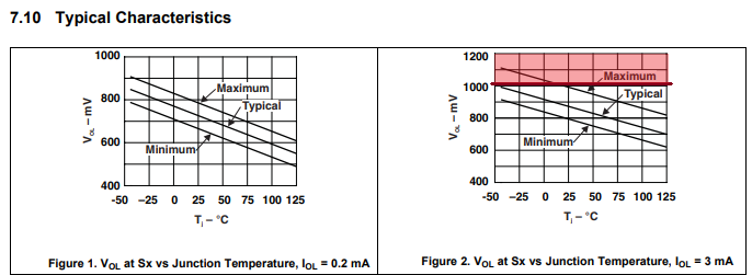
According to the data sheet with VCC 0f 3.3V (see below picture) the VIL (TYP) is 0.88V (and can reach even 1V) and I wand to connect it to LVCMOS 1.8V Bisdirectunal FPGA pin


The problem is that the LVCMOS 1.8 VIL Max Voltage is 0.35 x 1.8 = 0.63V which is below VIL of the P82B96 device.


Can you recommend solution/device that will enale me to interface the P82B96 that works with VCC of 3.3V to LVSMOS 1.8 bidirectunal pin

P82B96.docx

Thanks,

Shlomi

  • Shlomi,

    We are out of the office at the moment but will try to get back to you later this week.

    Max

  • Hi Shlomi,

    For mismatches in I2C driver low-level output and receiver low-level input, a common solution is to put a buffer between components. In this case, is sounds like translating between a 3.3V bus to a 1.8V bus would also be helpful. I would recommend a Level-Translating Buffer such as TCA9803 be placed between P82B96 (Vcc > 2V) and the LVCMOS device (Vcc = 1.8V) to allow the two to interface. 

    For reference, TCA9803 has the following characteristics:

    Low-level output voltage will be low enough to interface with LVCMOS with Vol = 0.63V

    Low-level input voltage when operating at 3.3V is high enough to interface with P82B96 Vol Max of 1.0V

    Let me know if this solution sounds good or if there are other constraints that may require a different approach. 

    Regards,

    Eric

  • To add an additional point to Eric's post, the B side of the TCA980x should NOT be connected to the P82B96 S side. Only A side of the TCA980x would support connection to the P82B96 S side. An alternative solution would also be the TCA9509 where A side can face the 1.8V logic side.

    -Bobby

  • Hi Bobby & Eric,

    Can you please explain Why: 

    “Only A side of the TCA980x would support connection to the P82B96 S side”

    Thanks,

    Shlomi

  • The TCA980x datasheet states that B side cannot connect to other buffers on the static voltage offset side. This is because B side senses the current inorder to detect which side is driving low, static voltage offset buffers may not pull enough current during contention and instead will confuse the low detection algorithm of the device making it oscillate.

    -Bobby

  • Hi Bobby,

    Can you please approve the attached connection between the P82B96TD to UltraScale FPGA using the TCA9803 device.

    UltraScale LVCMOS18  Input/Output levels are marked in the attached picture.

    Thanks,

    Shlomi

    P82B96 using TCA9803.docx

  • Hi Shlomi,

    The diagram you shared looks good. All Vol - Vil combinations are compatible based for typical datasheet specifications and the placement of of pull-up resistors is correct. I will advise that there is possibility for incompatible output voltages from the P82B96 under certain operating conditions; large current sink requirements and cool junction temperature (Iol = 3mA and Tj < 25C). Please check your design with Figure 7.10 on P82B96 datasheet to make sure the system can tolerate these conditions. I would suggest carefully choosing the pull-up resistor values to ensure that this sink current is not required of the device. Let me know if you have questions about this.

    From P82B96 Datasheet:

    TCA9803 Max Vil = 0.99V when Vcc = 3.3V. P82B96 Vol must be below this value (red line above).

    Regards,

    Eric