This thread has been locked.

If you have a related question, please click the "Ask a related question" button in the top right corner. The newly created question will be automatically linked to this question.

TPS65987D: unsuccessful power swap with TPS65987D

Part Number: TPS65987D
Other Parts Discussed in Thread: TUSB320

I'm using TPS65987D to interact with an Android phone via a USB-C in 2 modes: UFP & DRP at 2 different scenarios. As the board does not have its own power source, the device is configured as UFP (dead battery mode) when it's first connected to an Android phone. It relies on the phone power to power on the board. When another external power source is applied, we want the TPS65987D to do a PD PR_Swap to source in order to act as a power source to the phone (i.e. charging the phone). The problem is, as soon as the swap occurs, there is little current going to the phone which causes it to output a message "device is slowly charging ..".

The following programming procedure was done prior to the swap:

Upon boot up (in dead battery mode) with power provided by the phone:
1. clear dead battery flag
2. write to Tx Src Capability reg

Upon another external power was applied:
3. write to Global Config reg
4. write to Port Config reg
5. write to Port Control reg
6. send command SWSr to phone to swap power (attempt to make the phone a sink and our board a source)

After step 3, the USB connection to phone is lost. After step 6, the power swap appears to take effect as the phone starts seeing signs of incoming charging as follows:

a) brief flashing screen and then charging icon show up
b) message prompts with "Device charging slowly .... for faster charging, use the charger that came with your phone. Make sure cable isn't damaged."

In reality, the USB connection is lost and the phone draws very little current. We measured the total consumption at the input where the external charge was applied, the current is only 150 mA (including the board and the phone, if it draws anything at all).

This behavior is not a lot different than what we expected. We would have expected that, after the power swap, the phone would become a sink while still maintaining data host (DFP) whereas our board would becomes a source while retaining data role as UFP, just like before the swap.

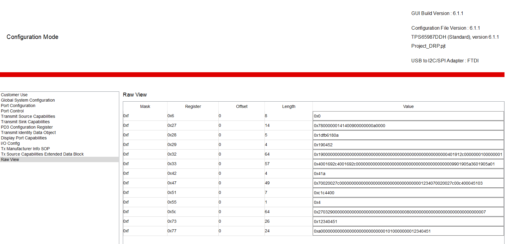
Can you please help pinpoint what went wrong with my set-up? I'm trying to attach App Custom Tool project that we based on to program the device. However, the site rejected it saying file type not permitted or mime type dose not match the file content. I'm now just sending a picture of the raw view instead.

Thank you in advance to help me to solve this issue.

  • Hi Daniel,

    Unfortunately, a PR Swap will result in a reset to change the roles for the PD controller so this behavior is expected. I will talk over with my team to see if there may be other options. Also, I do not see any images of you configurations, you will need to make sure you have the appropriate PDO's available for your smartphone. Could you try uploading the configurations again or possibly trying to attach the .pjt file to the thread?

    Thank you,

    Hari

  • Hi Hari,

    Thanks for your response.

    I understood and accepted that, a change in configuration (from UFP to DRP) will result in a reset. A brief disconnect from the USB port is expected.

    The problem is, after the power swap occurs, here are what happened:

    1. The phone withdraws power and the TPS65987D becomes a source (this is expected)

    2. The TPS65987D output a voltage of only 4.2V at the VBUS end going to the phone (this is NOT expected, should be ~5V as the input voltage at PP_HV2 is ~5.1V)

    3. The phone shows only 150 mA current draw from VBUS and sends a notification message "device is charging slowly ..."  (this is NOT expected)

    Point #2 above is what I found out today. The voltage is well below specs, so maybe there is some hint to this problem. I don't know why it sags so much even without the load from the phone.

    I measured all the voltages around the chip (schematics attached here) and all of them appear normal except the VBUS when the device acts  as a source. When it is a sink, the VBUS given by the phone is normal 5V.

    PD_schem.pdf

    I'm attaching the .pjt file here for your view. Also attached pictures of some key registers for a quick look.

    3771.Project_DRP.pjt

  • Hi Daniel,

    I took a quick look at your schematic and I think there might be an issue. I see that you have attached a voltage divider circuit with the 2 resistors on VBUS2, is there a reason you want to do this? It might be limiting the voltage output. I would recommend taking a look at Pin Functions section of the datasheet and going through the different pins to make sure they are all configured as recommended. You can also check out section 6.5, Power Supply Requirements and Characteristics, and see if those pins are meeting the required conditions and not out of range. 

    As for the project file, those configurations seem fine to me.

    Thank you,

    Hari

  • Hari,

    The pair of resistors on schematics (R63,R64) serves as voltage divider to 3.3V level to interrupt the MCU.

    We figured the current across them 0.0625 mA (5V/80K) shouldn't be a loading factor. We took them out anyway following your recommendation and nothing has changed as a result. Input voltage from the phone is 5V before the power swap, and becomes 4.2V after the swap.

    I forgot to mention one thing on schematics. The pair of resistors that defines ADCIN1 (R31=194K, R29=100K) was there at the beginning to form the value ADCIN1 = R2/(R1+R2)=0.34. This value together with SPI_MISO=0 was defined for boot mode pin strapping for device to enter BP_ECWait_Internal while in "dead battery mode". Our intention was to use our MCU to configure the chip through a series of I2C transactions. However, we couldn't get it to work so we changed the boot strap to ADCIN1=0.24 (BP_NoWait, Configuration 2, which is UFP only). So the actual value of R31 on the board now is 316K (to make the ADCIN1 ratio = 0.24). Hence, after the boot sequence, the TPS65987D goes straight to APP with UFP configuration. That goes in line with our board main function (battery-less device, get power from the phone to perform its main tasks) and it works fine.

    However, our board also supports another function which is, passes charge to the phone when an external power source comes to play. When this extra power source comes aboard, the MCU perform a series of I2C transactions to re-configure the TPS65987D to DRP mode, send power swap to source, etc. to pass the charge to the phone. That's where our current issue comes up.

    I'd like to seek your opinion with the following questions:

    1. What do you think about our strategy given our application as mentioned? Perhaps we should have started with DRP configuration in boot strap sequence rather than starting with UFP, then later changed to DRP? Or maybe it may take a while for the chip to reset and settle down before accepting a power swap?

    2. If we wanted to start with the DRP configuration (same as the one set up by the App Customization Tool we sent you), should we choose the Boot Mode Pin Strapping with SPI_MISO=0, ADCIN1=0.34 as originally intended before loading a series of patch commands? (which corresponds to BP_ECWait_Internal, Infinite Wait in Table 5 section 8.4.1 as in the datasheet).

    3. If we want send PTCd command, how do we extract the binary file (saved in App Custom Tool) into a series of 64-byte sequence as required input data?

  • Hi Hari,

    Did you have a chance to read my post above ?

    At present moment, I really want to try the patch method (using those 4CC patch commands right after boot) to configure the device as DRP from the get-go. 

    My problem is I don't know how to convert the binary file to a string of hex bytes to be used in my C-based program using I2C write function.

    The I2C write function requires the data portion (after slave address, register address, byte count) to be arranged in an array of bytes (in hex). Since the 'PTCd' (Patch Download) command requires 64 bytes as input data at a time, I'd imagine we shall send as many commands as it takes. However, given a binary file, how can I extract it into a series of 64-byte arrays to be used in my I2C write function?

    I guess my immediate need would be how to answer this question as a key to solve my charging issue. And I'd appreciate very much if you could help me through this. Thank you.

  • Hi Daniel,

    This app note should help answer your question. Figure 3 shows how to generate the binary file necessary to a firmware update over I2C.

    http://www.ti.com/lit/an/slva972a/slva972a.pdf

  • Hi Adam,

    Thanks for the app note.

    In order to do the patching commands, I changed the board configuration to BP_ECWait_Internal (ADCIN1 to 0.34). After booting up from dead battery mode, we used the MCU to load the patch commands as recommended (PTCs, PTCd, PTCc). However, the power swap behavior was the same as before, i.e. changing the application configuration with straight I2C write to appropriate registers.

    In other words, the power swap appeared to occur as I observed the following symptoms:

    1. The phone app showed the change from output current (-300 mA) to input current (200 mA), which was very little (the app name is Ampere)

    2. The output voltage from our board to the phone (VBUS) was only 4.2 V

    3. The transition from 5V input voltage (from the phone) to 4.2 V output voltage (from the internal PP2 switch) is INTANSTANEOUS

    Compared with the behavior from the EVM module:

    1. The phone app showed 1100 mA, which is expected.

    2. The VBUS voltage is ~5V (also from internal switch PP2), which is expected.

    3. There was a gap of 384 ms of the transition from input voltage to output voltage (5V -> 0V (384 ms) -> 5V)

    The 2 waveforms are attached.

    It appears that in my case there is something strange that makes the power switch PP2 not behaving as it should. It's not the problem of a specific chip as I tried on all the boards and they behaved the same way.

    Can you think any possibility that may cause this behavior of the chip? 

    Your help would be greatly appreciated.

    Thanks,

  • Hi Daniel,

    Is there a way to isolate/remove the 5V source that is connected to PPHV for the PD controller, and instead use a dedicated bench supply? The capture resembles a constant current scenario where the maximum current level is exceed, and to counter, the Rdson is increased, dropping the output voltage. However, I don't believe this is from the TPS65987D because the device has a 640uS timeout before opening up the FET. Since you see the voltage constant without a drop, don't believe that the PD controller is causing the voltage drop.

    Also, the fact that it is instantaneous is incorrect. Do you clear the dead battery flag once the patch has been successfully loaded and power boots up on the system?

    Would you also be able to read the status of register 0x26 during the above event?

  • Hi Adam,

    You are right. I was able to isolate the external 5V source and VBUS (we found a wrong part was used in between so we removed it for now). The result proves to be much better.

    There are no more voltage droop at the output of the PP2 switch and there is a gap of transition for VBUS (5V -> 0V (440ms) -> 5V) just like the behavior on the EVM.

    However, the current though much better (in the range of 700 mA) we'd like it to bring it up to the capability of the source (minus some used on our board which is about 300 mA).

    We wrote to the register Tx Source Cap (address 0x32) as (from LSB to MSB):

    0x01, 0x00, 0x00, 0x00, 0x01, 0x00, 0x00, 0x00, 0x2c, 0x91, 0x01,
    0x04, 0x00, 0x00, 0x00, 0x00, 0x00, 0x00, 0x00, 0x00, 0x00, 0x00, 0x00, 0x00, 0x00, 0x00, 0x00,
    0x00, 0x00, 0x00, 0x00, 0x00, 0x00, 0x00, 0x00, 0x00, 0x00, 0x90, 0x01, 0x00, 0x00, 0x00, 0x00, ...

    which is something like in this picture:

    How do we set up (beside the Tx Src Cap reg above) so that the phone can draw up to maximum capability (which is around 2 A according to the specs)?

  • Hi Daniel,

    Glad that was able to fix the issue.

    The only other option would be what pullup resistor is advertised for implicit contracts. This is controlled in the port control register (0x29).Make sure that the Type-C current is set to 3A as shown in the following image. That is the only other option for voltage/current advertisement.

    If this is set to the 3A setting, then the TPS65987D is advertising the maximum amount of current, and the phone is limiting the amount of current that it is drawing.

  • Adam,

    Actually we have 3A (strongest pullup) setting on Port Control reg (0x29). If that's the only other thing as far as the TPS65987D can do, then we ought to take a look at other possible causes such as the source ability (we use a TUSB320 to interface with the external power source via USB-C), or there might be a HW bottleneck somewhere from our board to the phone connector (there is a daughter board which connects to our board through a flex cable and connects to the phone via a USB-C plug). 

    Before closing this issue, I'd to ask you this all-important question because it will help me to decide the best architecture using the TPS65987D for my specific application:

    So far, we are using the method of booting (from dead battery mode because our board is BATTERY-LESS) with:

    1. pin strapping (SPI_MISO=0; ADCIN1 = 0.24) to get power from the phone and make the TPS65987D go straight to application mode with the default Configuration 2 (UFP).

    2. After that, as part of initialization routine, the MCU programs the device over I2C with registers such as Tx Src Cap (0x32), Clear Dead Battery Flag, etc.      EXCEPT  the 3 key registers that will re-configure the device to DRP mode: Global System Config (0x27), Port Config (0x28), Port Control (0x29).

    3. When an external charger is applied to the board, the MCU programs the above 3 registers and issue the command to do power swap to charge the phone.

    Using the above 3-step strategy gets us by so far to make the power swap happen. However, there are some undesirable effects:

    a) Because there are some programming procedure in step 3 between the charging cable insertion to the actual swap, there is some lag time which is not so smooth. Instead, we'd prefer to do only one swap command upon the charge cable insertion.

    b) There are only a few registers to be programmed in step 2. We only programmed the registers that we "thought" it would be necessary when the device becomes a source later. That's not a sure-fire approach as we'd like. The fact that we couldn't achieve current draw > 1A as opposed to what's seen on the EVM might have something to do with this. Therefore, we would prefer to program the exact configuration (DRP) as we set up in the Application Customization Tool.

    To solve a) and b), we think that the only way to go is to configure the device with the Patch Bundle Update tasks approach using the binary file generated by the tool. We did try this method by changing the boot strap pins to (SPI_MODE=0; ADCIN1 = 0.34) and successfully loading the patches. HOWEVER, here's our problem: As soon as the last command (PTCc) is completed, the device re-configure itself as DRP (which is expected), the VBUS voltage keeps toggling from 5V -> 0V -> 5V -> 0V ... endlessly. We think that might be a normal interaction between the 2 DRP devices (phone and our board) until they settle down (by chance?) with one becoming a DFP and the other UFP. But the problem is our board is a battery-less device, which depends totally on the phone's power to function. As soon as it loses power (period when VBUS = 0V), all data on the RAM of the TPS65987D is lost, so is the entire patch just loaded. When data is lost, it becomes a UFP just like at beginning, drawing power from battery to boot from "dead-battery" condition, VBUS would re-appear with 5V again. After that the TPS65987D re-boots to PTCH status, gets patches loaded again and re-configures as DRP again, which starts to negotiate the initial role with the phone again, which causes VBUS to turn 0V. This cycle repeats itself endlessly.

    My questions:

    1. Is there a way to make it come up as DRP and settles itself as UFP without going thru the process of initial negotiation over the role with the phone?

    2. If we implement an extra flash in our system to pre-store the patch, can the device will configure automatically as DRP (with UFP role initially) so we can avoid the process of loading the patches over I2C from the host and the inevitable process of re-configuring itself after that? 

    We'd appreciate your help very much.

    Thanks,

  • Hi Daniel,

    Answers to your questions below:

    1. No, if you wish your device to be a DRP, it must go through the negotiation process before initially settling as a UFP. There is no way to be a DRP and always come up as a UFP. This would make it a UFP

    2. You can use an external flash to load the configuration, but it would be redundant update the flash image from an external EEPROM as well as through I2C commands.

    If you want to have multiple configurations within one flash image, would recommend using the APP config functionality. Can follow this E2E post for integrating it into your project file.

    https://e2e.ti.com/support/interface/f/138/t/871307