Part Number: DS90UB948-Q1
Other Parts Discussed in Thread: DS90UH949A-Q1, DS90UB921-Q1, DS90UB947-Q1
Hello,
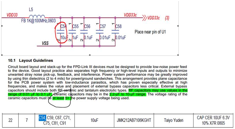
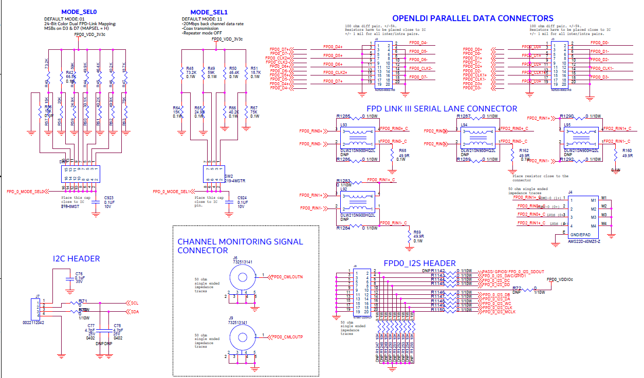
Regarding this DS90UB948-Q1 deserializer, I have designed FPD III to OLDI deserializers for LVDS, RGB, HDMI signals.
Totally three different deserializers in my design, for three serializers inputs (DS90UB947-Q1 for LVDS; DS90UH949A-Q1 for HDMI; DS90UB921-Q1 for RGB) which are coming from a vehicle dashboard silver box unit.
I am attaching the schematic of my design and would like to have your review comments and/or any suggestions.
Thanks in advance.
Regards,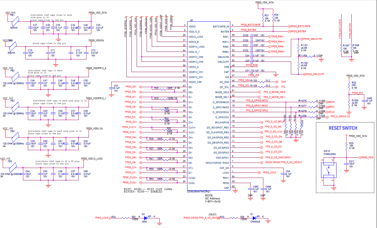
Pradeep. S