This thread has been locked.

If you have a related question, please click the "Ask a related question" button in the top right corner. The newly created question will be automatically linked to this question.

DS90UR124: Receive data error

Part Number: DS90UR124
Other Parts Discussed in Thread: DS90UR241

LVDS-OpticalFiber-MB-V1.3.pdf

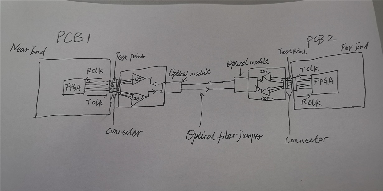
There are two chips ds90ur124 and ds90ur241 on the board, which are connected to the optical fiber module for long-distance transmission. Ds90ur124 and ds90ur241 chips are also used in the remote board card, and the optical fiber module is connected.

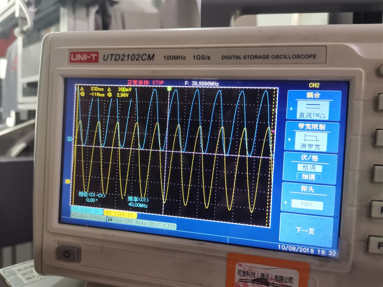
In Figure 2, the blue line is the transmission clock of 241, with the frequency of 40MHz, and the yellow line is the receiving clock of 24 pin output of 124. The transmitting clock is stable, and the receiving clock swings left and right (the period of the waveform seems to be unchanged). Because the bandwidth of the oscilloscope is 100MHz, the waveform seen is a sine wave, not a square wave.

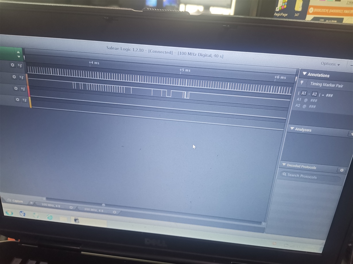
The logic analyzer in Figure 3 shows that the first signal detects one of the data lines of 241. The second signal is a receiving data line of 124。

 Lock status of 124:

There are two chips on the board, ds90ur124 and ds90ur241. Lock is high when only 124 chips are working. When the two chips receive and transmit at the same time, 124 can not receive data.

1、Please help to analyze the reason.

2、It is normal to measure the sending clock with an oscilloscope, but the receiving clock of 124 shows jitter with an oscilloscope. Is it normal?

  • Hello Zhang,

    Could you please send a block diagram for this system so we can understand the connections?

    Best Regards,

    Casey 

  • Working state: board 1 ----> board 2, a large amount of image data; board 2---->  board 1, a small amount of state data; the transmit and receive clocks are 40MHz, the transmit clock is provided by FPGA, and the receive clock is received by FPGA.

    Question 1: when the single board 1 receives the status information of board 2, it is normal, but the receiving clock has jitter. Is this jitter normal?

    Problem 2: when board card 1 sends data to board card 2, board card 2 can receive normally, but at this time, board card 1 cannot receive state data from board card 2 normally. At this time, the receiving clock of board card 1 also has jitter, which is roughly the same as the state described in problem 1. Please help to analyze the failure reason of receiving data?

  • hello,

    pls confirm:

    1. if disable board2 -> board1 direction, the link board1 -> board2 works normally?

    2. if disable board1 -> board12direction, the link board2 -> board1 works normally?

    3. if both directions are enabled, both links can't work and jitter is observed in receivers' PCLK pin? It is abnormal the high jitter is observed in PCLK pin.

    if yes, it could have cross-talk inside these two channels, it could be from optical module, or the on-board pcb layout. 

    regarsd,

    Steven