This thread has been locked.

If you have a related question, please click the "Ask a related question" button in the top right corner. The newly created question will be automatically linked to this question.

DS90UH948-Q1: 0x34 & 0x4B affect Vos?If we want to keep the original Vos, what should we do

Part Number: DS90UH948-Q1

Dear All

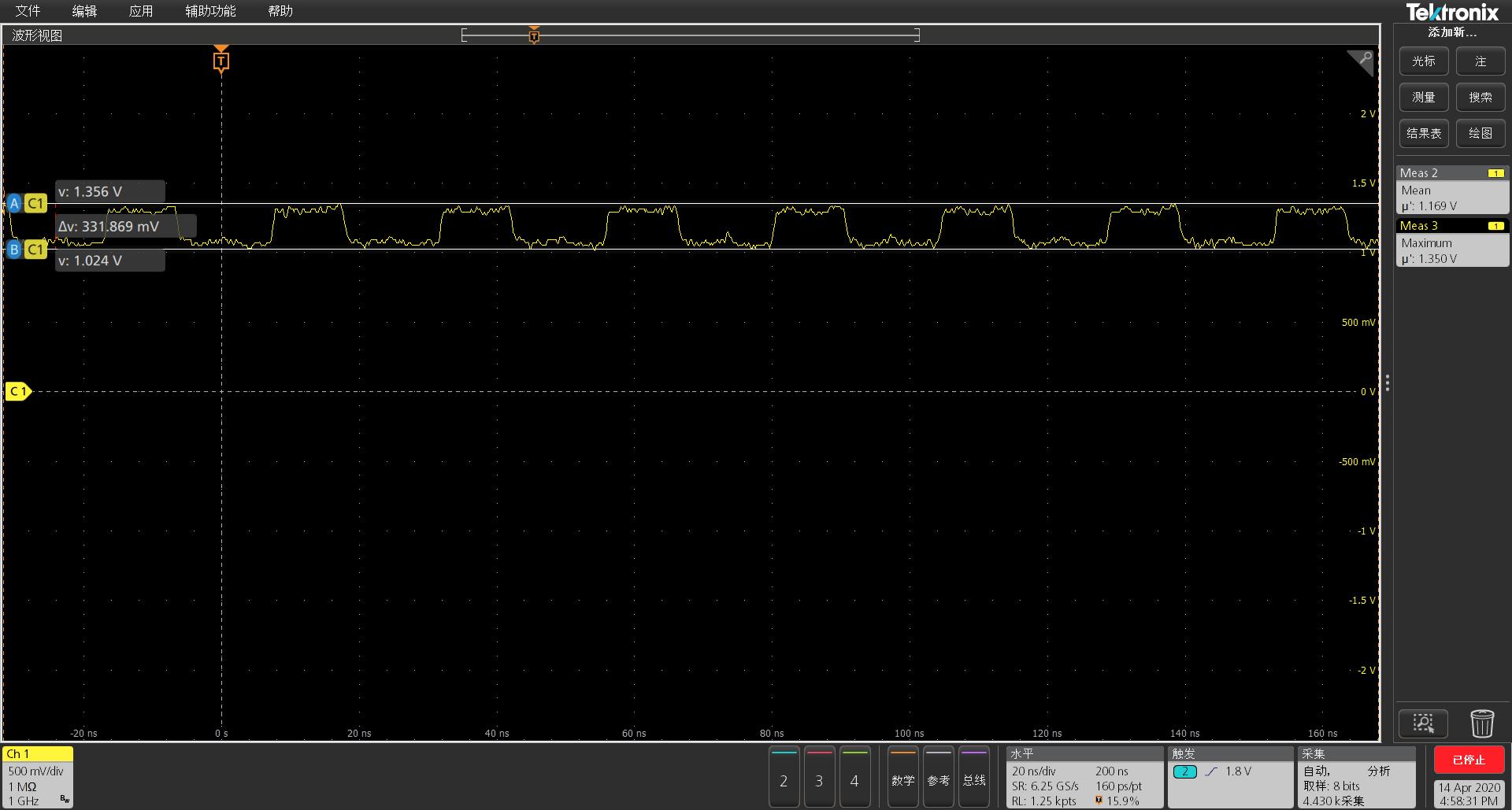
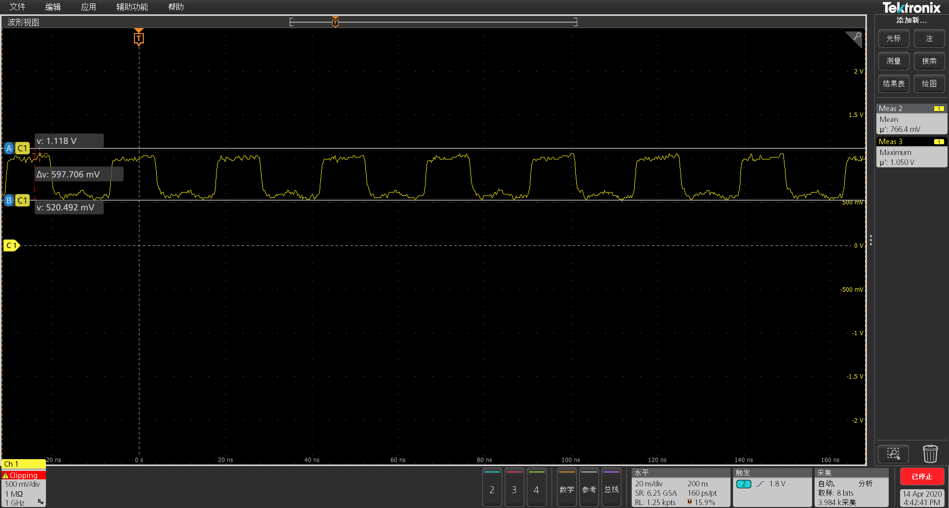
Related to the last question, we improved the swing amplitude after setting, but we found that this change changed the value of Vos (from the original 1.1V to 0.8V, SPEC = 1.125 ~ 1.375V).
Will the following statement change Vos?
step1. 0x34[1:0]=01 //port0
step2. 0x4B[1:0]=11
step3. 0x34[1:0]=10 //port1
step4. 0x4B[1:0]=11

At the same time we investigated the value of the current register
Addr = 0x34 , Value = 0x02
Addr = 0x4B , Value = 0x03

Will the default parts of 0x34 & 0x4B affect Vos?
If we want to keep the original Vos, what should we do
Thanks in advance~
I hope you can get through the epidemic as soon as possible。加油!
  • Hello,

    Is this measurement from a TI EVM or from a custom board?

    Thanks,

    Casey 

  • Hello,

    This is measurement from a custom board (948 #37_CLK1-> common mode choke->test point)

    Thanks,

    Aihua 

  • Hi Aihua,

    Yes changing register 0x4B will change the LVDS output VOS. The default is 190mV typical voltage swing (single-ended) and changing LVDS_VOD_Control to 11 will change the LVDS output to - 375mV typical voltage swing (single-ended). Your script to change each port separately is correct.

    Regards,

    Michael W.

  • Hi Michael,

    The following are the specifications required for our screen(Differential signal):
    We need both VOD Output voltage swing (differential) type = 750mV(we must use this swing to ensure that the swing = 200mV entering the chip inside the screen), and we need to keep Vos at type = 1.2V, how do we write our script~
    If the above requirements cannot be achieved, what should we do to meet the requirements of the screen...
    Thanks in advance.

    Best Regards,

    Aihua.

  • The specifications required for our screen(Differential signal):

    Differential input high threshold RXVTH max= 200 mV RXVCM=1.2V
    Differential input low threshold RXVTL min= -200 mV RXVCM=1.2V

    Input differential voltage |VID| =200 to 600 mV

    Differential Input Common Mode Voltage RXVCM min=1.0V type= 1.2V max=1.4 V

  • Hi Aihua,

    The LVDS drivers output there signal with a single ended common mode voltage of 1.2V.  This is called VOS in the datasheet. To meet the the input differential voltage then set the VOD setting to the highest level.

  • Hi Michael,

    Whether 0x4B bit [7: 2] = 0x00 or = 0x02 will cause the change as shown below.
    If not, which of the 0x4B default bits caused Vos to change, can the detailed configuration be shared?
    Thank you
    Best regards,
    Aihua.
    Figure1.
    Figure2.
  • Hi Aihua,

    When you are measuring this are you terminating the + and - lanes together using a 100 Ohm terminating resistor? What type of probe are you using?

    Regards,

    Michael W.

  • Hi Michael,

    We have used a 100 ohm resistor in the terminal. The probe model for testing the above waveforms is Tektronix TPP1000 1GHz Probe 300V CATII 3.9pF / 10Mohm. Usually, the probe for testing differential signals is TDP1500 Differential probe 1.5GHz (Range 850mV ~ 8.5V)
    Yesterday we did another survey on software.
    Figure1: 948register 0x34 & 0x4B value
    Addr = 0x34 , Value = 0x02
    Addr = 0x4B , Value = 0x03
    Figure2: 948register 0x34 & 0x4B value:
    Addr = 0x34 , Value = 0x01
    Addr = 0x4B , Value = 0x08
    From the above register comparison, it can be found that, ignoring the adjustment of the swing amplitude, 0x4B [7: 2] of Figuer1 should be 0x02 by default but set to 0x00.
    Is this the root cause of changing Vos?
    Thank you.
    Best regards,
    Aihua.
  • Hi Aihua,

    Did you read the value of 0x08 in register 0x4B or did you write that? Please do not write to reserved registers. when probing the signal are you ensuring that your ground loop is small?

    Regards,

    Michael W.

  • Hi Michael,

    Because it is difficult to connect to TI's website recently, I'm sorry for the late reply.
    The above values are read from the register. We have ensured that the ground loop is very small during this test. Are there any requirements for this?
    0x4B [7: 2] See the RW bit in the style book. Will the reserved bits be overwritten when 0x08-> 0x03?
    We gave the following instructions to the software,
    -----------------------------------------------
    step1. 0x34[7:0]=00000001 //选择port0
    step2. 0x4B[7:0]=00001011
    step3. 0x34[7:0]=00000010 //选择port1
    step4. 0x4B[7:0]=00001011
    -----------------------------------------------
    and the picture is the result of the final test:
    948 CLK1
    948 CLK2
    948 D3
    please see if this is possible.

    Best regards,

    Aihua.

  • Hi Aihua,

    "Will the reserved bits be overwritten when 0x08-> 0x03?"

    No this is fine.

    in the two pictures you attached the common mode voltage is ~1.2V which is correct.

    Regards,

    Michael W.