This thread has been locked.

If you have a related question, please click the "Ask a related question" button in the top right corner. The newly created question will be automatically linked to this question.

TPD4E05U06: TVS Diode S-parameter port mapping

Part Number: TPD4E05U06
Other Parts Discussed in Thread: ESD224, TPD1E05U06

Hi,
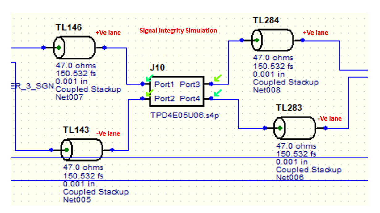
I have received the S4P file for the TVS Diode, I connected it to the PCIE +Ve and -Ve lanes. I see that strong connectivity between port 1&3 and 2&4 as shown in fig. I am confused, how do i port S-parameters to +Ve and -Ve TL's. Please find the below schematic, is it right? if not please share the port mapping for +Ve and -Ve lanes.
I read the conversation on TVS Diode port mapping it said that other end of the output should be NC but if we use in that way it is basically an OPEN.

Looking forward for the earliest reply.  

  • Hi,

    Welcome to E2E!

    I do not see a schematic attached to the post. Would you be able to share the schematic in question?

    As far as the what each port is for, the input ports(Port 1 & 2) correspond to the data signals before passing through the D+/D- pins of the TPD4E05U06. The output ports(Port 3 & 4) will be the data signal after the insertion loss due to the capacitance of the TPD4E05U06. None of these ports correspond to the NC pins of the TPD4E05U06 as the NC pins are not internally connected to the device.

    Best regards,

    Andy Robles

  • Hi Andy,
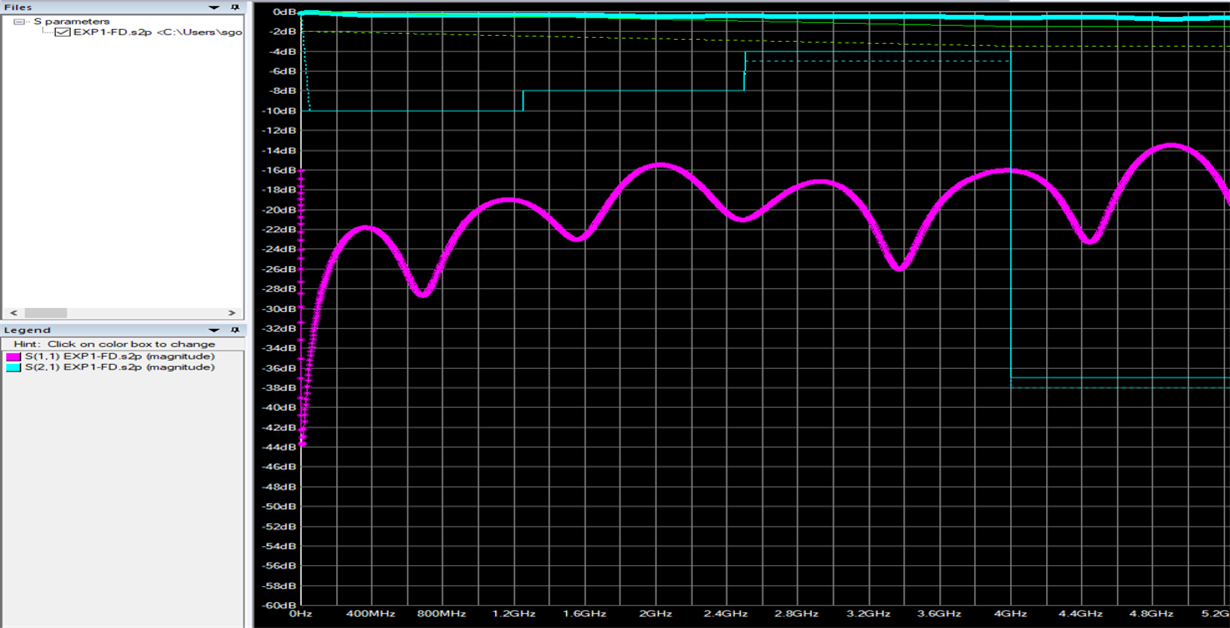
    PCIE Gen 2.0 TX is not complaint in both time domain and Frequency domain if we use TVS Diode in the circuit but if remove the TVS Diode then PCIE TX is complaint. It is quite strange, length of TL's is so small and tried various configurations with terminating but still not able to complaint. 

    Please find the attached schematic, any feedback is appreciated! 
    Thanks
    Sachin

  • Hi Andy,
    I wanted to follow up inregards to the previous S-port mapping question, do you have any update?

    Thanks

    Sachin

  • Hi Sachin,

    In the post you tagged we had an issue with the model which could be that the same issue we are having here. Instead of using Port 1 and 2 as the inputs and ports 3 and 4 as the outputs can we flip the model to have Ports 3 and 4 be the inputs and have Ports 1 and 2 be the outputs.

    Did this fix the issue or show a different behavior?

    Best regards,

    Andy Robles

  • Hi Andy Robles, 

    What it doesn’t say is what to do with the outputs 3&4 or input 1&2 or vice versa.  Where does it go, how is it routed on the board or how to simulate it in a circuit.  studied guidelines on TI site

    and tried various things in signal integrity simulation, but it doesn’t tell me how to hook it. Please see the schematic below and also attached SImulation schematic and plots with and without diode. 


    Please see below plots of freq domain parameters and ported as you mentioned earlier.

    Fig1: Schematic used for PCIE SI Simulation: 

    Fig2: Without TVS Diode: TX is COMPLAINT if i remove the TVS Diode and its related TL's(which is a very small segment though).

    Figure 3: With TVS Diode: I have performed Freq domain Analysis with input 3&4 and 1&2 as output and vice versa, either way TX is NON COMPLIANT. 

    Looking forward for reply and any feedback is appreciated!

    Thanks

    Sachin

  • Hi Sachin,

    The input ports are the D1+ and D1- pins of the TPD4E05U06. The output ports are also the D1+ and D- pins of the device, but will have the insertion loss from the ESD device. The output pins are the continuation of the signal trace and should be routed to the next components on the TX signal line. An example of a TDR can be found in the following application note: ESD224 HDMI® 2.0 Compliance and Protection

    Section 2.1 talks about how the bandwidth was measured on the device which the same applies to the TPD4E05U06. Only difference is that the ESD224 had an input pin and an output pin, and the TPD4E05U06 the I/O pins are both the input and the output. Section 2.2 has an example of the TDR for the ESD224, but the same applies for the TPD4E05U06.

    Best regards,

    Andy Robles

  • Hi Andy,

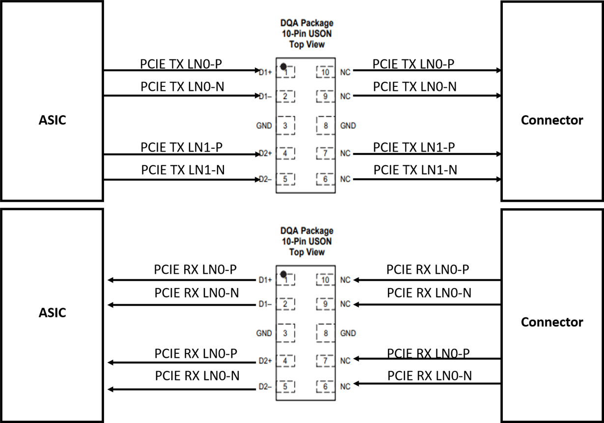
    1. In that case: 10pin DQA package has 4 pins not connected and also, read couple of other explanation in TI Site, which says NC mean not connected internally in package. Then how does output pins hook into the signal pairs?  

    2. However, In reference to your above explanation and with observation of application notes of ESD 224 (FIG 1) example, I have updated TPD4E05U06 (TVS Diode) schematic (FIG 2) and also, replicate s-parameter port mapping for circuit simulation (FIG 3) , if it is correct and if it goes well, then implement on board.
    It would be really great, if you could comment or suggest if i am wrong? Please see attached.

    FIG1: 

    FIG2: 

    FIG3:

    Thanks

    Sachin

  • Hi Sachin,

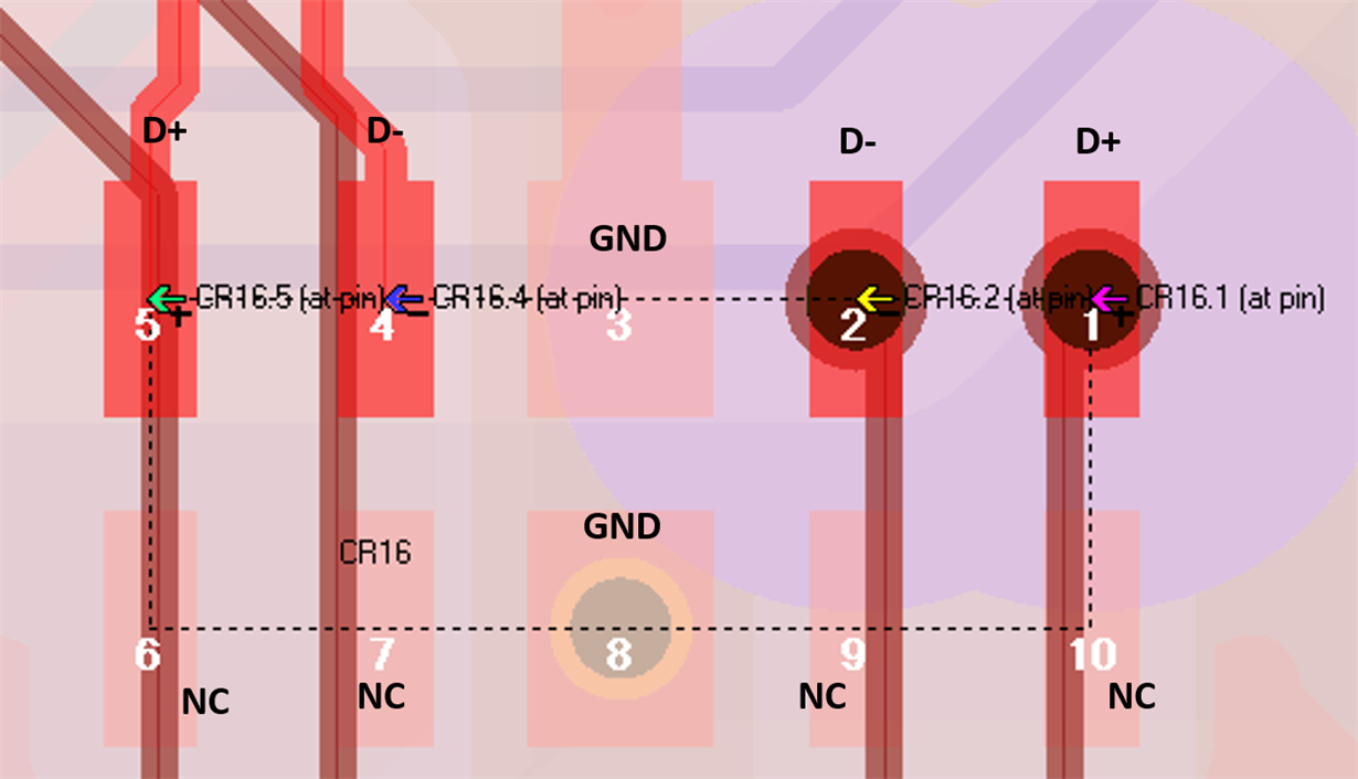
    The TPD4E05U06 does have 4 pins not internally connected. The NC pins are not internally connected to the device so whether anything is connected to these pins will not affect the functionality of the device. Since they are not internally connected they can be used for straight through routing in the layout. The D+ and D- pins of the TPD4E05U06 is the same as the I/O pins of the TPD1E05U06 (same device as TPD4E05U06, but single channel). The signal trace simply passes over the I/O pin the same way it would the D+ and D- pins in the TPD4E05U06.

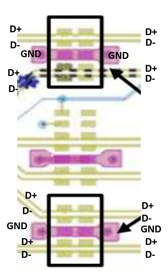
    Since the NC pins are not internally connected you can route through them if it helps for the layout, but you don not have to route through them. Below the trace in red is acceptable, but routing through the NC pins is also acceptable.

    The schematic for the simulation looks good and it should model the insertion loss from the device.

    Best regards,

    Andy Robles

  • Hi Andy,
    Thanks for your quick response. So basically, below two solutions for schematic & routing are acceptable.

    Solution1: FIG1& FIG2:

    Solution2:Alternate: FIG 3 & 4

    FIG1:

    FIG2:

    FIG3:

    FIG4:

    Thanks

    SAchin

  • Hi Sachin,

    I can't really see the whole layout, but from i can see the layout in Figure 2 is NOT okay. From what I can see the there's a trace that only goes to D+/ and D- pins, but the signals does not continue through the pin. If Figure 2 layout is like the image below then it is NOT okay.

    The data line from the connector should go straight to the D+/D- pins of the TPD4E05U06 and then from the D+/D- pins to the ASIC like Figure 3 and Figure 4 in your last post.

    For more details on optimal ESD layout please refer to the following application report: ESD Protection Layout Guide

    Best regards,

    Andy Robles

  • Hi Andy,

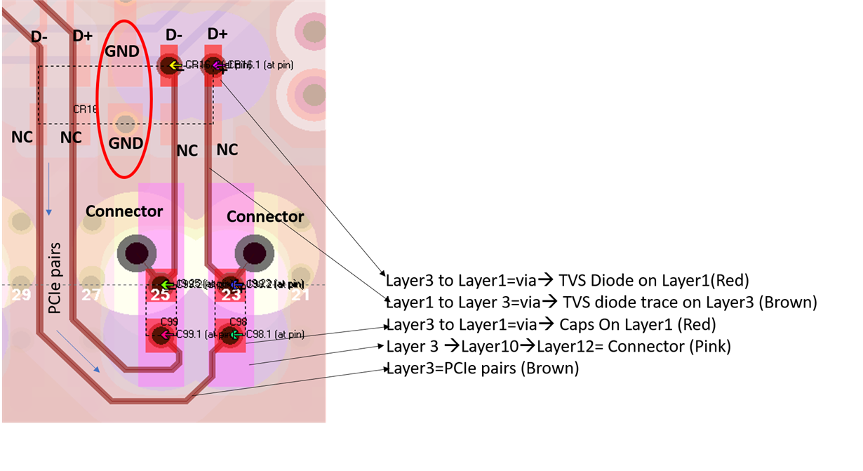
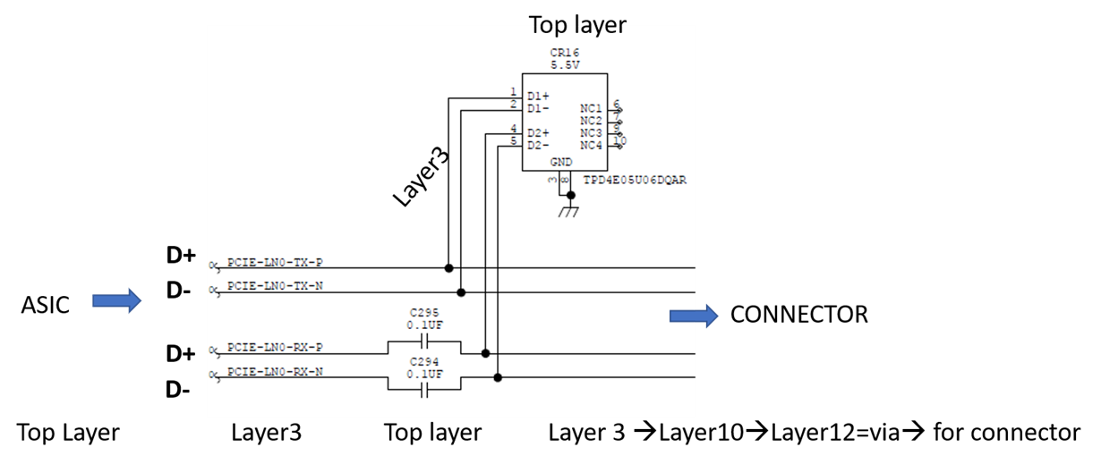
     Please find the attached schematic and layout for TVS Diode. 

    We have routed it parallely as show in above figures and while SI Simulation, TVS Diode placed it in series. Please comment!!

    Thanks

    Sachin

  • Hi Sachin,

    It is highly recommended for the TVS diode protection pin to be in between the ESD source and the protected IC. In your layout I see that the connector has two paths. One path is from the connector to the TVS diode and the other path I believe is from the connector to the protected IC. The TVS diode should not be branched out like that. Please refer to section 2.1 in the ESD Layout Guide for more details.

    If you have further questions about the layout you can reach out to me through email at a-robles@ti.com

    Best regards,

    Andy Robles

  • Hi Sachin,

    I will be closing this thread as we will continue this conversation over email.

    Best regards,

    Andy Robles