This thread has been locked.

If you have a related question, please click the "Ask a related question" button in the top right corner. The newly created question will be automatically linked to this question.

DS80PCI102: eye diagram fail

Part Number: DS80PCI102


Hi Sir,

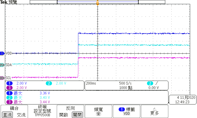
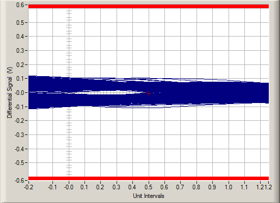
could you help confirm whether this schematic is correct? because the customer to verify the eye diagram is failure and could not be open.

Please let us know the reason and learn from you. look forward to you reply.thanks.

attached is schematic and eye diagram.

sr-n707-g0a-1_20201007.pdf

  • Hi Tommy,

    Reviewed this schematic and please below note some comments:

    1). VDD_SEL: This pin needs to be either tied to GND or float. In this schematic, 20K ohm resistor is used to GND. Please change this 20k Ohm resistor to 0 ohm.

    2). Given ENSMB is tied to GND through 1K ohm resistor, this means we are controlling the part through pin settings.

    a). VOD_SEL pin 17: This pin is a test point. It means this pin is float. Please note table 3 of the DS80PCI102 data sheet. We need to make sure VOD selection and device EQ settings(table 2 of the data sheet) provides adequate VOD and EQ gain for the media attached on both output and input. Please note table 3 and table 2 of the data sheet for detailed settings and make sure you have options or settings to enable different settings for these two pins..  

    3). Rate Pin#13: This pin is float - Auto rate detection with de-emphasis. It would be good to have the flexibility to change this setting. This means we should be able to float or tie this pin through 20K or 1K ohm to GND.

    4). Noticed you are using R124 and R125 on input B side. Please replace these with AC coupling caps. If TX side connected to input B does have AC coupling Cap then we can leave these. Normally, in PCIe application TX provides AC coupling Caps. Additionally components such as R124 and R125 provides parasitic and degrades signal integrity.

    In summary, please refer to table 2 and 3 for detailed EQ and VOD/DEM settings to make sure there are settings to enable different options/setting. Given the scope shot you provided, it seems perhaps EQ and VOD/DEM pins may not have the optimum settings.

    Regards,, Nasser 

  • 1). VDD_SEL: This pin needs to be either tied to GND or float. In this schematic, 20K ohm resistor is used to GND. Please change this 20k Ohm resistor to 0 ohm.

    But I debug 0 ohm,funtion is fail ,I measure VDD1,VDD2 =3.3V,Is it OK?

  • PRSNT# :This pin is tied to Gnd,Will it affect PCI-E Gen3 timing?

    Does such a function need to use EEPROM?

  • Greetings,

    1). PRSNT# can be tied to GND and will not affect Gen3 timing.

    2). Using EEPROM is not a must. EEPROM or SMBus interface can allow register changes. I think the issue you are seeing could be related to EQ and de-emphasis settings. Please refer to the summary section of the earlier response i had sent.

    Regards,, Nasser

  • I reference 

    3.3-V Mode of Operation
    1. Tie VDD_SEL = 0 with 1-kΩ resistor to GND.
    2. Feed 3.3-V supply into VIN pin. Local 1.0-µF decoupling at VIN is recommended.
    3. See information on VDD bypass below.
    4. SDA and SCL pins should connect pullup resistor to VIN

    3.3k pull high


    5. Any 4-Level input which requires a connection to "Logic 1" should use a 1-kΩ resistor to VIN

    why VDD=3.3V,not 2.5V

  • Hi Ling Shou,

    I just checked this on one of the evaluation boards and VDD is 2.5V given the setup you have noted. 

    1). Did you check this on different parts? Maybe the part is damaged somehow.

    2). You can get one of the evaluation boards and check this as well but this seems to be working fine and as expected.

    Regards,, Nasser

  • 2). You can get one of the evaluation boards and check this as well but this seems to be working fine and as expected.

    Can  you give  EVB sample for me?free? 

  • Greetings,

    Please discuss this with your local TI sales/contact.

    Regards,, Nasser

  • I set 

    ENSMB=0,PRSNT#=0,VOD_SEL=F,DEMA/B=0,RXDET=F,SD_TH=F,EQA1\EQB1=R,EQA0\EQB0=0

    why I debug RATE=R is pass,auto select gen1/2 and gen3 with de-emphasis is fail

    How auto select use ?

  • Greetings,

    When RATE is set to auto - RATE pin FLOAT - device detects whether incoming rate is Gen1/Gen2 or Gen3. When it detects Gen3,  output amplitude follows input peak to peak signal. Further, device enables de-emphasis.

    On the other hand, when RATE pin is set to R, device VOD follows input peak to peak signal AND de-emphasis is not enabled. In this case, device is operating in linear mode. 

    It is possible when RATE pin was FLOAT we may have been over equalizing the output signal,

    Regards,, Nasser