This thread has been locked.

If you have a related question, please click the "Ask a related question" button in the top right corner. The newly created question will be automatically linked to this question.

DP83867IR: DP83867IR

Part Number: DP83867IR

Hello,

  I have issues getting loopback to work with the DP83867IR.  My setup has a FPGA driving the PHY, given current limitations I am forced to 10 MBps and 2.5 Mhz (25M would likely work). MII interface NOT RGMII

  MDIO register read write works fine from the FPGA

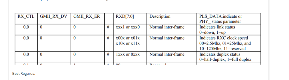
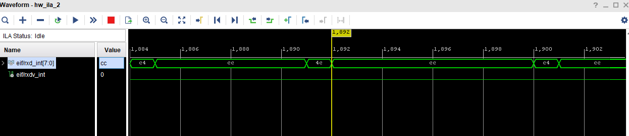
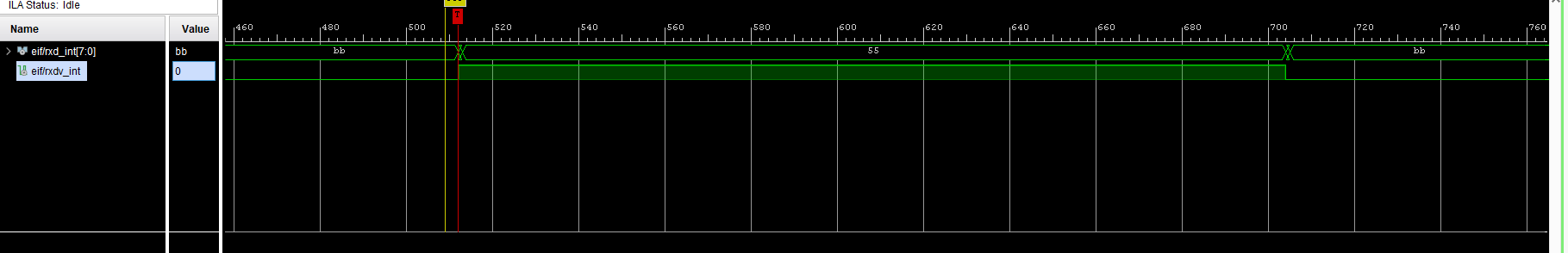
  Sending data on the TX interface, not observing RXDV high.

   I have not been sending the ADDR/DATA  0x001f/0x8000, 0x001f/0x0x4000, from another thread this does not seem to be required. 

https://e2e.ti.com/support/interface/f/138/t/684210


MII Loopback

  0x0000/0x0100   Full Duplex, 10 Mbps, Auto Neg off

  0x000D/0x001f, 0x000E/0x00fe,0x000D/0x401f, 0x000E/0xe720   Write 0xE720 to Extended address 0xfe

  0x0/0x4100         Turn on MII Loopback

Also tried 

  0x0000/0x0100   Full Duplex, 10 Mbps, Auto Neg off

  0x000D/0x001f, 0x000E/0x00fe,0x000D/0x401f, 0x000E/0xe720   Write 0xE720 to Extended address 0xfe

  0x0016/0x0004  Digital Loopback

  0x001f/0x4000   SW restart

Thanks for any help

George


  • Hi George,

    After programming the device for digital loopback, can you read back the following registers:

    • 0x0
    • 0x1
    • 0x10
    • 0x11
    • 0x16
    • 0x6E
    • 0x6F

    Thank you,

    Nikhil

  • Hi Nikhil,

      I realized in my debugging that The part I'm trying to interface to is a QFN package that does not support MII/GMII and I'm forced to RGMII @125Mhz.  At least with my current configuration I don't seem to be receiving the GTX clock.  Since the QFN and QFP package share the same register set I'm trying to figure out what features/configuration I can set with the QFN part.  For instance, I can set the speed in register address 0x0 to 10 Mbps that results in a RX clock of 2.5 Mhz.  Speed is not that important in my particular application and I will not be driving this part with a MAC.  My code for the MDIO interface is working fine, and otherwise I'm just trying to use the phy as a data path to an external device.  I'm guessing that I need to set 0x32 bit 7 to RGMII, that may get the GTX clock working.  Since I am not connecting to a network, auto-neg, link alive etc are not important. 

    - Can I run RGMII with speed set to 10 Mbps so that I get a 2.5 Mhz RX clock (I'm using that clock for the MDIO interface currently).  Such a asymmetric data rate could be a problem I would imagine especially in loopback.  If TX is forced to run at the GTX rate of 125 Mhz, what are my loopback setup options?

    - Right now I'm trying to loop back through the PHY to verify my FPGA code, shallow loopback, "MII" loopback set in address 0x0.  Given that the QFN part is restricted to RGMII, there are likely a lot of register settings that are not allowed or ignored.  We should have used the QFP package, but I'm trying to work around with what we have.

      Right now I have

    0x0      0x4100

    0x1      0x7949

    0x10    0x5848

    0x11    0x2b02

    0x16    0x0000

    Will need to modify my verilog a bit to get 0x6e and 0x6f

    Hoping you can get me the correct register settings so that I can see some evidence of loopback.  I was not planning on having to run at 125Mhz so any settings where I can reduce the MAC (FPGA in my case) to PHY transfer rates would be very helpful.

    Thanks

    George

  • I believe the answer will be:

    - I need to source my MDIO interface clock from elsewhere/not return clocks from the phy

    - Since I am forced into RGMII mode, both RX and GTX/TX clock will be 125 Mhz.  

    George

  • Hi George,

    In RGMII mode, you may still force the PHY to a lower speed. However, in RGMII mode, TX clock is an input to the PHY, the MAC clock will have to be adjusted accordingly. RX_CLK will automatically change with speed selection, 25 MHz for 100 Mbps and 2.5 MHz for 10 Mbps. You may force 100 Mbps speed by setting register 0x0 = 0x2100, and you may force 10 Mbps speed by setting 0x0 = 0x0100.

    For the purposes of this debug, let's try to establish a working digital loopback setup. After bootup and configuring the desired speed setting, can you set register 0x16 = 0x4 (set digital loopback), and provide a register dump of the same registers above? 

    Thank you,

    Nikhil

  • Hi Nikhil,

      I have a couple more values for MII loopback

    0x00    0x6100

    0x01    0x7949

    0x10    0x5848

    0x11    0x6b02

    0x16    0x0000

    0x6e   :: 0x080f

    0x6f    :: 0x0104

    RGMII interface 

    Current loopback setup

    Adr      Data

    0x00 :: x6100

    0xfe  :: 0x3720

    0x32 :: 0x00d0

    Will try digital loopback next

    Still have not seen RXDV go high

    Thanks

    George

  • Hello,

      Following this post 

    https://e2e.ti.com/support/interface/f/138/t/684210

    Write

    Addr   Data

    0x0    0x2100

    0x16  0x0004

    0xfe   0xe720

    0x32  0x00d0

    0x1f   0x4000

    Readback

    0x00    0x2100

    0x01    0x794d

    0x10    0x5848

    0x11    0x6c02

    0x16    0x0004

    0x6e   :: 0x080f

    0x6f    :: 0x0104

    I believe this is report link up, but still no RXDV returned

    Thanks for any help

    George

  • Hi George,

    It looks like register 0x32[1:0] = 00. This corresponds to RGMII receive and transmit clock is aligned to receive data. Is the MAC or are the PCB traces configured to provide skew data? Based on the RGMII spec, there must be a TX or RX skew, this could be why you are not seeing any valid data transfer. If you are unsure about the MAC settings, you may try adjusting 0x32[1:0] for different combinations of TX and RX alignment and skew settings. 

    Thank you,

    Nikhil

  • Hi Nikhil,

      I had planned on tuning the design at some point, but currently I'm trying to see any evidence of proper operation on the TX/RX data interface.  By design my RX path has ~2.5 ns of clk/data skew which should be sufficient.  My TX path did not have skew and previously the PHY was configured for 0 ns skew so I modified my register setup so that:

    0x0    :: 0x2100
    0x16  :: 0x0004

    0xFE  :: 0xe720

    0x32  :: 0x00d2

    0x86  :: 0x00f0

    0x1f  :: 0x4000

    • 0x0      ::   0x2100
    • 0x1      ::   0x794d
    • 0x10    ::   0x5848
    • 0x11    ::   0x6f02
    • 0x16   ::   0x0004
    • 0x6E   ::   0x080f
    • 0x6F   ::   0x0104

    Thanks for any help

    George

  • Hello,

    Thanks for the follow up. Replies on E2E are delayed due to end of year holidays. We will get back to you by Jan 7.

    -Regards

    Aniruddha

  • Hello,

      Still no evidence of loopback, some things I have tried

      - My current implementation has 2.5ns of RX skew and programmed 2.5ns of TX skew through Phy registers.

      - Tried adding 5ns extra TX skew with Xilinx MMCM

      - Tried non loopback case to see if LED outputs will display TX activity (Link LED0 turns on when I try digital loopback), LED2 does not show TX or RX activity

      - Verified txclk, txen timing on scope (with added skew)

      - rxd path is showing both 0x4 and 0xc, 0x4 indicating 25 Mhz which is correct, but bit3 would be indicating the part switching in/out of full duplex mode????

    Thanks for any help

    George

  • Hi George,

    We are looking into your question and will provide feedback by 1/7.

    Thank you,

    Nikhil

  • Hi George,

    Can you please confirm what is meant by "rxd path is showing both 0x4 and 0xc"? Is this a register you are reading and if so, which register?

    Thank you,

    Nikhil

  • Hi Nikhil,

      I was referring to the RXD[3:0] RGMII data from the PHY.  I have yet to see RXDV assert but see 0x4/0xc returning from the Phy.  I got the below data from another forum post

    Thanks

    George

  • Hi George,

    Where are you seeing the values 0x4/0xC returned from the PHY? Is this a register reading/which register?

    It looks like the attachment links are broken (see below), can you try reattaching? 

    Thank you,

    Nikhil

  • Hi George,

    Is this issue seen when swapping out and using different MACs and different PHYs?

    Thank you,

    Nikhil

  • Hi Nikhil,

      I am driving the Phy with a FPGA.  Our architects plan is to use a POE scheme to drive power/data to (and data from) an external peripheral.  This is not a true ethernet application, on the FPGA side I have a MDIO interface I coded up and a simple data path interface to RGMII.  Due to pinout restrictions and cable length this was deemed to be an acceptable solution.   MDIO reading and writing registers works fine, however as I have indicted I cannot get loopback to work. I can see the RXCLK change frequency as a result of register changes and RMW works so I can communicate with the Phy.

    My understanding is that I should be able to use the RGMII interface for raw data and that there is no data framing necessary.  The 0x4/0xc on the RXD interface is withut any external connection to the Phy ethernet pins.  Given this particular application, would you have any recommendations for register settings?

    Thanks

    George

  • Hi George,

    As a functional test, rather than sending packets from the MAC, can we try enabling digital loopback, and the PRBS generator? Packets will be generated along the MDI and digitally looped back to the RX pins. You should be able to observe packets on the RX pins with this setup. The following script may be tried:

    001F    8000    //Hard Reset
    0000    0140    //Force 1G Speed
    0010    5008    //Force MDI
    00FE   E720    //Loopback Control Adjustment, use extended register access sequence as you have before
    0016    0004    //digital loopback enable

    001F    4000    //Soft Reset
    0016    F004    //Digital loopback + Enable PRBS Generator
    0016    E004    //Enable digital loopback, Stop PRBS Generator

    Please let me know if you are able to observe RX activity with this script.

    Thank you,

    Nikhil

  • Hi Nikhil,

       That sequence results in the below trace.  I modified the 0x0000 write to 0x2100 for 100 MBps

       Getting 0xB when RX bus is idle, that indicates link up, 25 Mhz, full dup.

       The write to 0x0010, 0x5008 is something I have not attempted before.

       I don't see a TX data counter for this part so unclear how to prove that TX packets are arriving.

      Next steps?

    Thanks a bunch

    George


  • Hello,

      The issue I'm currently having is that is that return data is always 0x55.  This occurs in PRBS mode or in loopback mode with PRBS off.  Different transfer lengths with PRBS off show matching between the TX data path and RX so that would indicate that the TXEN and RXDV skew timing is correct.  TX data and RX data have the same skew as TXEN and RXDV  so I would think that this is not explicitly an issue with skew.  Does the constant x55 data pattern (same pattern in PRBS or digital loopback) have some meaning?

    Thanks

    George

  • Hi George,

    Upon further review of the register dump, it looks like register 0x10 = 5848 is enabling a reserved bit that is likely placing the PHY out of the desired operating mode. Can you try setting register 0x10 based on your need?

    • 0x10 = 0x5048 // auto-MDIX
    • 0x10 = 0x5028 // Force MDIX
    • 0x10 = 0x5008 // Force MDI

    Thank you,

    Nikhil

  • Hi Nikhil,

      Thank you and now I am able to RX data, however I'm still encountering issues

    - Writing 0x10 with 0x5008 (per suggestion above)

    - RX interface does not seem to be operating in RGMII, after testing loopback patterns and PRBS pattern, I'm not able to capture falling edge data

      - Have tried several skew values in register 0x86 [7:0], 0x32 = 0xd3 which should enable RX/TX delay and RGMII

      - Tried further skew using Xilinx MMCM, not able to affect RX data pattern

      - RX data always has 2 bytes of 0x55 preceding TX pattern (when not running in PRBS mode)

    Today I hope to get some of the RX data path signals on a scope to definitively determine if RGMII/DDR is working.

    Given that this part shares register set of a part with other interface options, is there some register setting I could be missing that could be confusing the RX/TX interface?  The only pertinent register I know of is 0x32 bit 7 =1

    Thanks

    George

  • Hi George,

    I want to confirm our current status:

    • You are able to observe both rising and falling edge of RX_Dx pins using PRBS and digital loopback
    • After setting register 0x10, you can now observe RX data from the MAC (without PRBS)
      • Falling edge data cannot be captured.
      • Changing RX/TX skew did not help

    Are the above statements all correct?

    Some follow up questions:

    1. Was both rising and falling edge of data observed during the PRBS setup?
    2. Does the MAC have capability to count packets sent/received and check for errors? With MAC sending packets to PHY and PHY looping packets back to MAC, can MAC count for errors? If the MAC is counting packets received and identifies no errors, the error may be in the data capture rather than data transfer. 

    Given Register 0x32 is showing bit[7] = 1, PHY should be in RGMII mode. 

    Thank you,

    Nikhil

  • Hi Nikhil,

      - For both PRBS mode and digital loopback mode, I see the lower nibble replicated onto the upper nibble in the RX datapath.  This happens regardless of RX skew setting or clock delay added via MMCM in the FPGA.  

      - I have verified that for TX I see data bits changing on the rising and falling edge of the clock.  Data/clock is aligned coming out of the FPGA and Phy is set for 4ns of skew @25Mhz clock (100 Mbps setting)

      - I'm using ChipScope on the FPGA side to view data after the input DDR I/Os  That is where I'm seeing the upper/lower data replication.

      - Tomorrow I should be able to get some debug probes to take a look at the raw data out of the Phy.  

    Since you indicate that 0x32 bit 7 is the only enable for RGMII (not sure why it would need to be enabled on a part that only supports RGMII) then it must be on my side.  Once I see the raw RX data signals I will know for sure if the RX interface is operating in RGMII mode.

    Thanks

    George

  • Hi Nikhil,

      I'm looking at the RXD bit 0 and the RXCLK from the Phy, running PRBS mode.  I cannot find a RXD[0] transition that is less than 40ns (clock period = 40 ns).  That is, I do not see RXD[0] transitioning on the falling edge of the clock.  I'm looking at pseudo random data, but can you think of any reason the why the interface would not be working in DDR mode/RGMII?

    Thanks

    George

  • Hi George,

    As a debug step, can we try the following configuration:

    • Connect DP83867 to link partner via MDI interface
    • Have link partner transmit data via MDI
    • DP83867 should output data on RX pins.

    In this configuration, no loopbacks should be involve. The DP83867 should not be connected to a MAC. This will just be a functional check of a link partner sending packets to the DP83867, and the DP83867 outputting packets on the RX pins. When probing the RX pins in this configuration, is falling edge data observed?

    Thank you,

    Nikhil

  • Hi Nikhil,

      Unfortunately I cannot do that.  For my application there is no MAC, we are sending raw data into the PHY from a FPGA.  This is point to point, raw data to/from one phy to another external device.  We are using the phy to simply modulate the raw data through a POE transformer to tx/rx our data and power to a remote device.

      At least what I have been trying to accomplish for a few weeks is to try to simply loop data back through the phy to prove out my TX/RX interface.  I wrote my own MDIO interface and that was simple.  The TX/RX interface should be even simpler but is causing endless headaches....

    Thanks

    George

  • Hi George,

    Please allow me to clarify. I would like to try an experiment where data is sent across the MDI (cable side RJ45 interface). Do you have a link partner available that can generate packets across the MDI pairs? When the PHY receives this information, it should generate packets on the RX pins to be sent to the MAC. Is falling edge data observed in this setup?

    Additionally, are you able to provide a schematic?

    Thank you,

    Nikhil