Other Parts Discussed in Thread: SN65DSI84
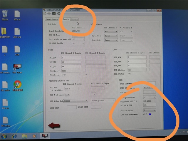
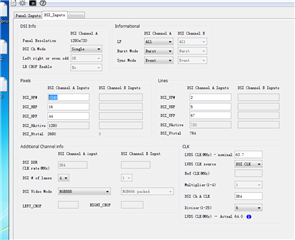
After power is applied and stable, How can we let the DSI CLK lanes to be in HS state and let the DSI data lanes be driven to LP11 state?.There is anything we should to do ?
Original question:

After power is applied and stable, How can we let the DSI CLK lanes to be in HS state and let the DSI data lanes be driven to LP11 state?.There is anything we should to do ?