


Other Parts Discussed in Thread: ISO1541, ISO1540
This post tries to explain in a simple way the basic operation of the ISO1540 and ISO1541 I2C isolators.
I hope you enjoy it. Kind regards, Thomas
Operational Principle of a Bidirectional Isolator (for LIN and I2C Interfaces)
Open-drain buses such as LIN and I2C have their signal lines pulled low when indicating an active data bit on the line. These busses work bidirectional, meaning either transceiver can communicate with another one using the same wire (Figure 1).
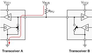
Figure 1. Transceiver A starts data transfer with transceiver B by pulling the data line low.
In systems with significant ground potential differences between bus nodes, galvanic signal isolation is required to prevent otherwise flowing ground currents from deteriorating the bus signal and causing data errors.
Signal isolators are however unidirectional, and it takes two of them to construct a bidirectional isolator. However, simply connecting the isolator inputs and outputs at both ends creates a closed signal loop that is prone to latch-up. In this case the isolator can pass a low signal but can never return back to a high-impedance state (Figure 2).

Figure 2. This simple trial of a bidirectional isolator will latch-up because of its closed signal loop.
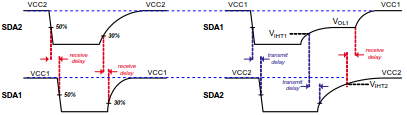
To prevent latch-up, the signal loop is split by a comparator which distinguishes between two different low levels, VOL1 and VOL2.
VOL1 is the output low level of an I2C transceiver. VOL2 is the raised output low level of the isolator at node A. the difference between the two levels is typically a diode forward voltage drop: .
The comparator distinguishes between VOL1 and VOL2 by comparing the voltages at its signal input with the voltage potential at its reference input which is set to (Figure3).

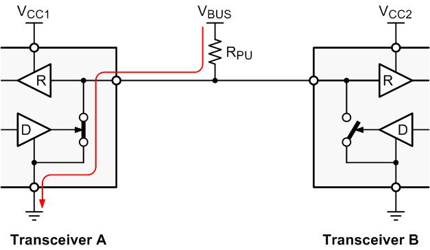
Figure 3. This bidirectional isolator splits the signal loop with a comparator and won’t latch-up.
OPERATION
During bus idling, when the bus is not actively driven, both isolator I/O ports are high-impedance.
When transceiver B pulls node B low, this low passes through the isolation barrier and activates switch S1. At this moment the isolator output at node A assumes VOL2 potential. Because VOL2 > VREF, the comparator output turns high. This high passes across the barrier leaving switch S2 open. Thus there is no interference between the input signal at node B and the open feedback loop output, S2.
Note that the isolator output at node A is so designed that VOL2 is lower than then input low-level thresholds of CMOS Schmitt-trigger inputs, VIL. This is necessary in order for VOL2 to be accepted as valid CMOS input low-level.
When transceiver B turns high-impedance, high (VCC2) potential lies at the isolator input B, which passes across the barrier opening S1. Node A now turning high-impedance, assumes high (VCC1) potential via pull-up resistor RPU1.
In the opposite direction, when input A is pulled low, the signal input of the comparator has VOL1 potential. Because VOL1 < VREF the comparator output turns low, thus closing S2 and turning output B low. The low is fed back across the barrier closing S1. Because node A is already at its lowest possible potential, VOL1, the feedback loop has no impact on the comparator input signal, and the comparator output remains high.
When the output of transceiver A becomes high-impedance node A will only rise to VOL2 potential as S2 is still closed. However, the change from VOL1 to VOL2 causes the comparator output to switch from low to high, thus opening S2. Node B then assumes VCC2 potential, which is passed as high across the barrier opening S1. At this moment the output of S1 becomes high-impedance allowing for node A to continue rising up to full VCC1 potential.
CONCLUSION
The dominant time (the time between the falling and the rising signal edge) of an input signal created by transceiver B must have the duration of at least one propagation delay through the isolator for the input signal to reach output A.
In the opposite direction however, an input signal generated by transceiver A must have a dominant time of at least the full round-trip propagation delay to ensure node A is fully released before the next falling edge.
Note: This simplified explanation does not take any bus capacitances into account. The bus capacitance both sides of the isolator in combination with the pull-up resistors form R-C time constants which typically exceed the isolator propagation delays. Hence, for a detailed timing analysis refer to the calculation examples of the respective interface standards, LIN or I2C.
