This thread has been locked.
If you have a related question, please click the "Ask a related question" button in the top right corner. The newly created question will be automatically linked to this question.
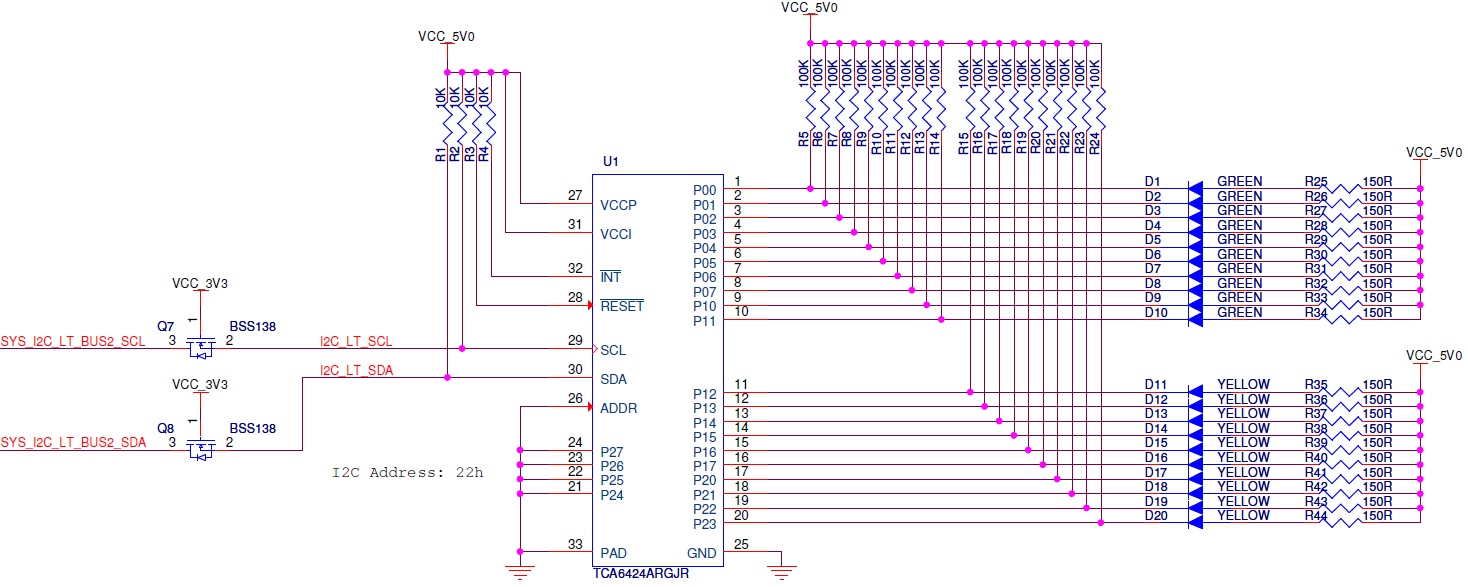
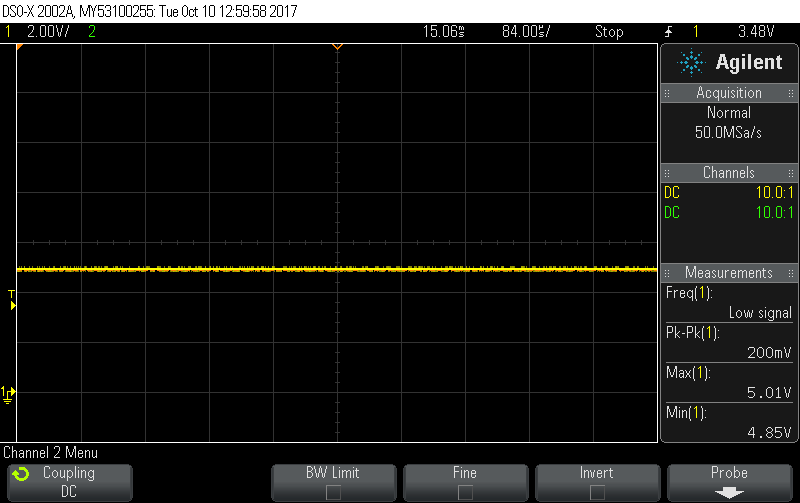
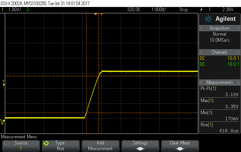
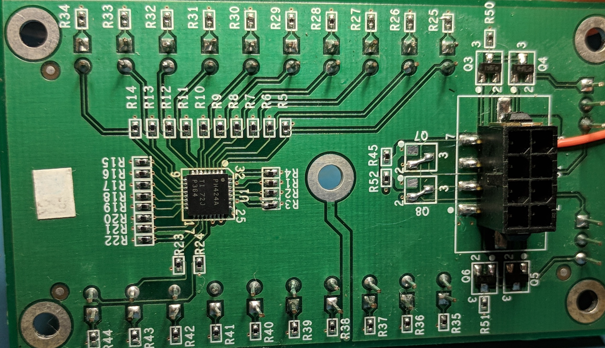
When we are performing the I2C scan, we are not able to detect the device. When we probed SCL and SDA pins it was found that the device is not giving an ACK. We have checked all the voltages and all of them are proper. Please find the snapshot of our design for your reference. Kindly suggest any solutions to this issue.
Hi Bobby,
1) We probed the o-scopes on the PIN 2 side of the FETS (Q7 and Q8).
2) FETs are their to act as level translators. FPGA is giving 3V3 level signals and the device needs 5V level signals as per our design. So the FETs perform the job of level translation and as it can be seen from the captures that they are working fine as expected.
--Shiva
Hey Bobby,
1) Yes, this is an issue that we are observing on multiple boards.
2) We probed directly at pin 28 (reset) and ensured that this pin is not holding low. It reads 5V/3.3V depending on the corresponding VCC we are supplying.
3) It is not possible to change the address by placing a pull up resistor on pin26 (ADDR) in our case as for doing that we would need to cut a pcb trace.
4) On the left of the mosfets, we have another translator before the FPGA which translates from 2.5V to 3.3V. We have checked its working, and it is working properly.
5) We also tested the chip without the mosfets. We changed Vcci/Vccp to 3.3V and removed the mosfets and shorted the pads of the fets 2 and 3 together. The same observation was recorded.
6) We could not check the current into VCCP as there is no other component between this pin and the voltage rail. Its connected through a PCB trace through which we cannot measure the current.
Thanks,
-Shiva
Hi Bobby,
1) We probed the RESET pin during the data transaction and observed that RESET is stable at a logic high level during the whole data transaction time. We also checked VCCI pin during the transaction time and observed that it was stable at 3V3 during the whole transaction time.
2) We probed the VCCI and VCCP pins to see the ramp up times. Following are the captures:
VCCI:
VCCP:
3) We have purchased it online from Mouser Electronics. Kindly find the high resolution picture of the device for your reference:
--Thanks,
Shiva