The latest release of the USB PD2.0 Specification (Version 1.2, March 25th, 2016), released as part of the USB3.1 Spec on the USB.org Developer Documents page, includes the new "Power Rules" that are also included in USB PD Rev 3.0, Ver 1.0a. As a result, Section 10 - simply named "Power Rules" - is identical in the PD2.0 and PD3.0 specifications.
The "Power Rules" in the PD2.0 Ver 1.2 refresh are intended to provide a more mathematical approach to providing power as a USB Power Delivery (PD) Source where the output current at every voltage is based on the maximum Wattage of the power supply. This change by itself makes a lot of sense when compared to the original "Power Profiles" put forth in the original PD2.0 Spec.
The hardest change for designers to understand, though, may be that the standard voltage levels to be offered have changed:
- Original USB PD2.0 Spec Voltages = 5, 12, and 20V
- New USB PD2.0 Ver 1.2 (and PD3.0) Spec Voltages = 5, 9, 15, and 20V
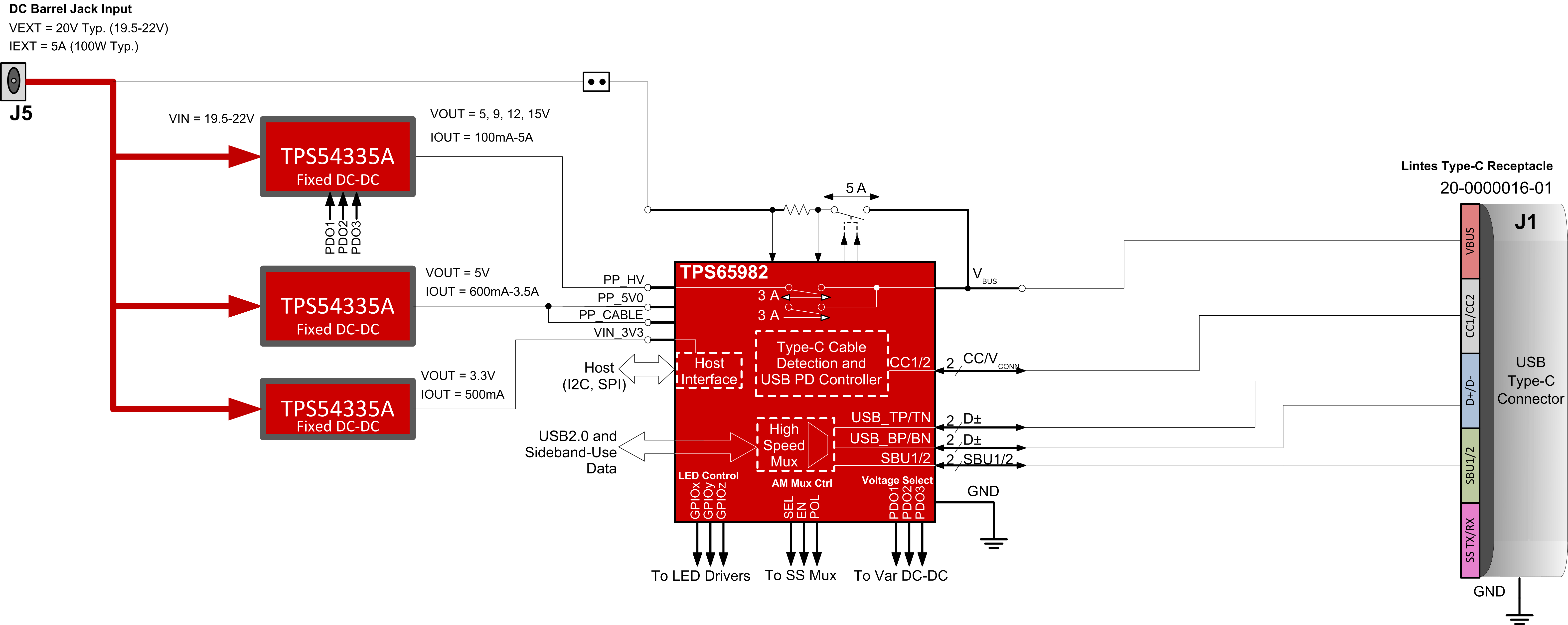
When studying the TPS65982-EVM, it is easy to see that this hardware cannot easily be modified to support 9V and 15V because the TPS54335A DC-DC buck converter that provides PP_HV is fixed at 12 Volts. Adding another external Power Path to the Mux seems like an additional burden on the designer, and adding more DC-DC converters will definitely add to the BOM cost.
Question: What is the simplest, cheapest solution to provide 9V and 15V using the TPS65982?
Answer: Keep the TPS54335A and convert it to a "Variable DC-DC Buck Converter" that can provide 9V and 15V! And you can still provide 12V for backwards compatibility using this method.
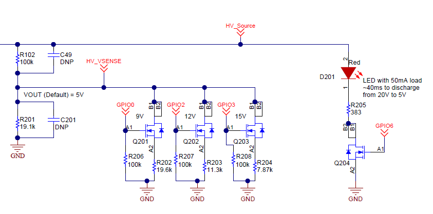
The block diagram of this new circuit is shown below:
By using the equation for VOUT of the TPS54335A, we can add resistors in parallel with R2 and control them with GPIOs of the TPS65982 that automatically turn on when a new high voltage PD contract is negotiated at 9, 12, or 15V.
VOUT = VREF * (R1 + R2) / R2, where VREF = 0.8V; R1 = 100kOhms; VOUT = default, 9V, 12V, 15V
There is a single R2 resistor that is always in the circuit which sets the default output voltage, where VOUT,default <= 9V. Although 9 Volts would work, a GPIO to create 9V would not be needed. So for the sake of creating an example and potentially reducing the BOM count even further, we will set VOUT,default = 5V and then R2 = 19.1k (after a typical resistance value is substituted for the ideal resistance calculated, 19.05kOhm)
Then calculate R2 three more times to solve for the other R2' values: R2,9V = 9.75k; R2,12V = 7.14k; R2,15V = 5.63k
Now, in the actual circuit R2 will be in parallel with new resistors to create the voltage, so we can call these R2X resistors R2A, R2B, and R2C where:
R2X = R2' * R2 / (R2' + R2)
Solving for R2X and substituting the closest lower standard resistor available, we get R2A = 19.6k; R2B = 11.3k; R2C = 7.87k
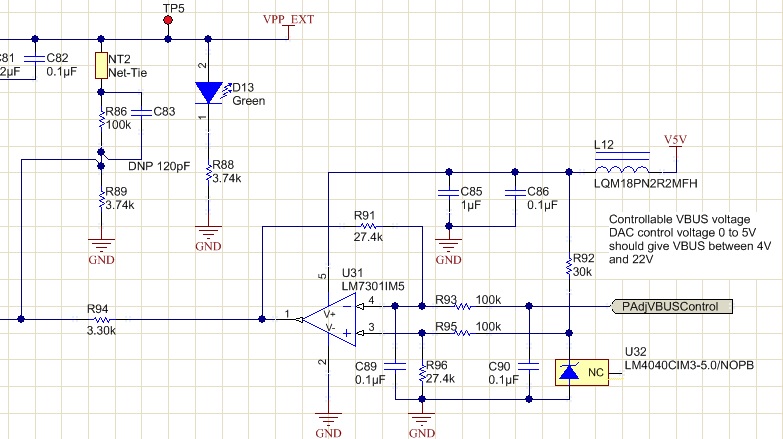
In the attached updated schematics of the TPS65982-EVM, all added components are annotated starting at 201 (R201 for resistors, D201 for diodes, Q201 for transistors, C201 for capacitors).
The following resistors are used in the modified TPS54335A voltage divider feedback circuit:
- R2 = R201
- R2A = R202
- R2B = R203
- R2C = R204
Finally, a diode D201 is added to "bleed" the voltage from a maximum of 15V down to 5V because the TPS54335A does not have the FCCM Mode as a feature and the bulk capacitors used to stabilize the output voltage will need to be discharged during negative voltage transitions at PP_HV (VBUS is automatically discharged by the TPS65982).
Another noteworthy change is the replacement of the PP_EXT FETs Q1 and Q2 with the latest version, the CSD87501L, a combined Back-to-Back 30V NexFET in a WCSP package that will support up to 5A to source 20V (100W).
The attached schematics can be used as a reference to refresh USB PD designs using the TPS65982 to support PD2.0 Ver 1.2 and PD3.0 voltages as outlined by the new "Power Rules". Now, your products can Source a wide range of standard PD voltages (5, 9, 12, 15, and 20V) with a simple design and minimal added components.