


If the USB PD "Power Rules" for PD2.0 rev 1.2 and PD3.0 is a new topic for you, I suggest reading my other post on the topic before this post.

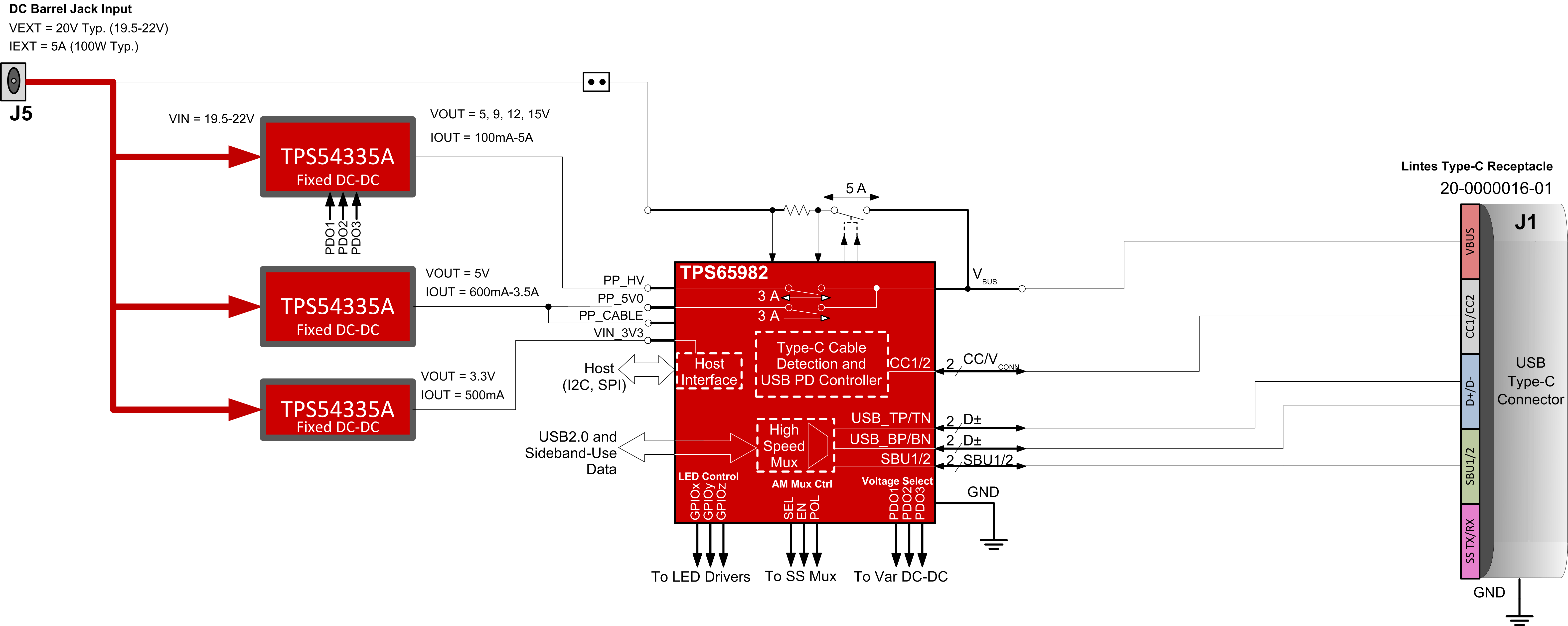
In the first post on this topic, it was easy to re-design the TPS65982-EVM for more voltages by keeping the TPS54335A in the design and simply converting it to a "Variable DC-DC" converter and controlling it the GPIOs of the TPS65982.
The Variable DC-DC buck converter can theoretically support as many different voltages as needed by the application, so a Dual-Role Port (DRP) that needs to sink power on the PP_EXT FET path of the TPS65982 should be able to deliver 9V, 15V, and 20V through the PP_HV FET path as a Source. Some applications will also need to provide 12 Volts to support legacy USB PD devices that only accept a 12V PD Contract.
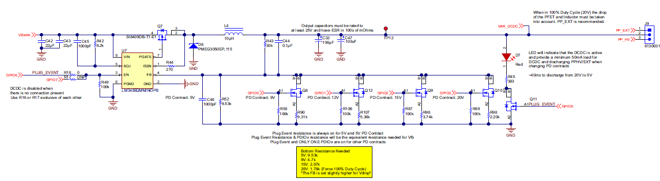
The problem with a USB PD DRP that needs to provide 9V, 12V, 15V, and 20V from a single DC-DC converter is that the DC Barrel Jack voltage is exactly 20V and most DC-DC buck converters cannot support 100% Duty Cycle operation.
The block diagram above shows the TPS65982 controlling the LM3489 as a Variable DC-DC buck converter to deliver 9, 12, 15, and 20 Volts through either the PP_HV internal high voltage path or the PP_EXT external high voltage path, while the path not used as a PD Source is used as to Sink power from VBUS. As a result, this design can be used as a Dual-Role Port (DRP) that is capable of being line-powered from a barrel jack or bus-powered over Type-C.
The attached schematic for this design shows the Power Path containing the LM3489 on Page 2 and the Type-C connector and TPS65982 PD controlleron Page 1. GPIOs 0-3 are outputs from the TPS65982 that switch in the correct resistor in the LM3489 circuit to deliver the appropriate voltage when a Source PDO contract is negotiated. The LM3489 can achieve 100% duty cycle because it is a Hysteretic PFET type of DC-DC buck controller, meaning that when 20 V is required, the PFET is driven on 100% of the time and is effectively a switch that is closed.
GPIO6 is also an output from the TPS65982 that is used to drive the EN pin of the LM3489 high only when a Type-C connection is present. GPIO6 simultaneously turns on LED D7, which is used to “bleed” the voltage from a higher voltage to a lower voltage when necessary. For example, the system may be delivering 20 V to a laptop which is removed and quickly replaced with a tablet that only needs 9 V to charge its battery. The TPS65982 automatically discharges VBUS to meet the USB PD specification, but if LED D7 were not present the PP_HV (or PP_EXT) node would be stuck at 20 V until it discharges naturally. This natural discharge could take seconds to minutes when an un-plug and re-plug event at the Type-C port could happen in as little as 1 second.
Certain DC-DC converter ICs can perform this “voltage bleed” automatically, and this feature is referred to as “output discharge” or “forced continuous conduction mode” (FCCM). For more details on FCCM as a way to remove LED D7 and save power, refer to the TPS53353 datasheet. The additional passive circuitry and connectors in not discussed in this post are the same as the TPS65982-EVM.
The major deviations from the TPS65982 to this design using the LM3489 are shown in a screen shot below, but all details are provided in the attached PDFs.
PMP20165-TPS65982+LM3489_Power_Delivery_pg1of2.pdf
PMP20165-TPS65982+LM3489_Power_Path_pg2of2.pdf
I hope this post is a convenient and useful guide for new designs, and please ask questions if anything is unclear.


