This thread has been locked.

If you have a related question, please click the "Ask a related question" button in the top right corner. The newly created question will be automatically linked to this question.

SN6505B-Q1: Output voltage equation and Input current

Part Number: SN6505B-Q1

Hello,

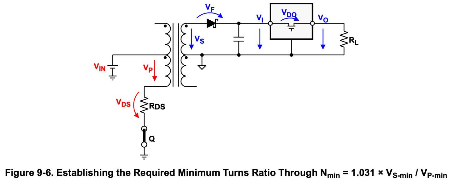
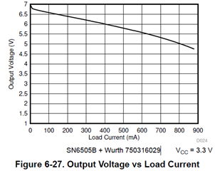
I would like to step-up 3.3V to 5V at a load current of 300mA. I want to estimate worst case output voltage or worst case input voltage for LDO and Input current consumption at full load. Do you have a formula for the same ? As mentioned in datasheet I want to use Wurth 750316029 as push pull transformer.

Also, 

The output voltage mentioned in the below graph regards Shottky diode drop as well or its just the secondary voltage before rectified diode ?

Thanks & Regards,

Manoj.

  • Hi Manoj,

    Thank you for reaching out.

    The datasheet provides an equation to calculate turns-ratio which uses worst-case parameters to determine turns-ratio for the worst-case test condition. Please refer to Equation (10) from datasheet, also copied below where VO-max and ID-max are the max output voltage and input current. You can use this equation to calculate VO-max after estimating ID-max.

    Assuming a worst-case efficiency of 85%, ID-max can be estimate as, ID-max = VO * IO / (VIN * Eff) = 5V * 300mA / (3.3V * 0.85) = 535mA. You can substitute this value in Equation (10) to calculate VO-max.

    The output voltage mentioned in the below graph regards Shottky diode drop as well or its just the secondary voltage before rectified diode ?

    The voltage before rectifier diodes is a pulsating DC voltage, hence, this is not referred in datasheet. The voltage shown in the graph is the final output voltage after rectification and filtering. Thanks.


    Regards,
    Koteshwar Rao

  • Hello Koteshwar,

    Thanks for the response. I would like to calculate Maximum output voltage of the transformer after rectification. I assume VO-max in the equation(10) refers to maximum output voltage of the LDO(based on the example & Eq -11). Could you please clarify the same ?

    Also,

    Do you have the part number of rectifier diode that is used to get the results in Fig 6-27 ? I believe in the Fig 6-27 the forward voltage drop of rectifier diode considered at 25 degC. Since i am doing worst case calculations from -40 to +125C, I would need this information. So that in any case the LDO (LP3869x/-Q1) I have selected would never go out of regulation unitl 300mA over full temperature range.

    Best Regards,

    Manoj.

  • Hi Manoj,

    Thanks for the response. I would like to calculate Maximum output voltage of the transformer after rectification. I assume VO-max in the equation(10) refers to maximum output voltage of the LDO(based on the example & Eq -11). Could you please clarify the same ?

    Sorry, I should have clarified this. The only difference between the voltage after rectification and after LDO is the voltage drop across LDO, VDO-max. Please make VDO-max = 0V or remove this from the equation and the calculated value should be the output voltage after rectification. The below diagram graphically locates all these voltage parameters in the schematic.

    Do you have the part number of rectifier diode that is used to get the results in Fig 6-27 ?

    I understand the reason for asking for the diode part number. All the output voltage and efficiency curves are captured using default EVM configuration which uses the diode 1N5819HW-7-F. Thanks.


    Regards,
    Koteshwar Rao

  • Hi Koteshwar,

    Thanks for the response. I have few questions related to equation 10. I believe leakage inductance, winding DC resistance of the transformer and switching losses of internal mosfet of the DC-DC converter is not considered in that formula. if it is true, how much variation in output voltage that i can expect ??

    Regards,

    Manoj.

  • Hi Manoj,

    Thank you for following up with additional questions.

    The transformer correction factor in the equation (added as 1.031) already compensates for winding DC resistance. The product "IDmax * RDSmax" cover the conduction losses that occur in internal MOSFETs. While leakage inductance and switching losses do not directly impact the output voltage rather they impact the overall efficiency.

    This is the reason why these are not part of the equation for output voltage / turns-ratio. Thanks.


    Regards,
    Koteshwar Rao

  • Hi Koteshwar,

    Thanks for the information. Do you have any information regarding the power losses in the driver. I would like to calculate the power losses in the driver when the output current is 300mA.

    Best Regards,

    Manoj.

  • Hi Manoj,

    Yes, the power loss in device can be calculated using the drain current (ID) and RDS(ON). You can use the below equation to calculate power loss in device SN6505B-Q1

    PD = ID(avg) * [RDSmax ^ 2]

    where ID(avg) is the average input current and RDSmax is the maximum RDS(ON) value which is 0.31Ω according to the datasheet. ID(avg) is ~630mA (= turns-ratio * output current = 2.1*300mA). Thanks.


    Regards,
    Koteshwar Rao

  • Hello Koteshwar,

    Thanks for the response. I have calculated the power dissipation as per formula mentioned above. only thing i have changed is instead of considering 0.31Ω for RDS(ON),  I have considered 0.31*1.7= 0.527Ω for the calculation. since Rds(ON) mentioned in the datasheet is at room temperature and it wil increase as the temperature rises and I want to calculate the losses at 105 degC ambient temperature. So the conduction losses = 0.31*1.7*630=209mW. Then I have calculated Power dissipation of the device with the help of Junction-to-ambient thermal resistance = 137.7 °C/W.                                             Power dissipation at 105 ambient = (130-105)/137.7 = 181mW. I have considered 130 degC Junction temperature since the datasheet says min thermal shutdown temperature is at 135 degc(5degC margin). with this it looks like at input current of 630mA the device will be in Thermal shutdown mode. Is my understanding correct ? if this is true i might have to choose different driver IC for my application. Can you recommend some other driver from TI which can handle input currents of 700mA ?

    Best Regards,

    Manoj.

  • Hi Manoj,

    Thank you for your inputs.

    Please note that only the values specified in the middle column as typical are the values measured at 25C (see below screenshot from datasheet). The min/max values are the worst-case values considering temperature variation and part-to-part variation. Hence, I do not expect the RDS(ON) to be any more than 0.31Ω.

    I would also like to mention that 0.31Ω is the RDS(ON) when VCC = 2.8V while it is 0.25Ω when VCC = 4.5V. I expect the value to be in-between 0.25Ω and 0.31Ω when VCC = 3.3V. Therefore, RDS(ON) for VCC = 3.3V should never exceed 0.31Ω.

    The power loss or dissipation at 630mA current and RDS(ON) of 0.31Ω using the equation I shared in my previous post is, 61mW. You probably missed to square the resistance in calculating power loss / dissipation. With a power dissipation of 61mW, the difference between ambient and junction temperature is going to be 8.4C (= 61mW * 137.7C/W). This means that when ambient temperature is 105C, the junction is only going to be 113.4C.

    Please also note that the minimum thermal shutdown threshold is 154C as stated in the datasheet. The device doesn't go to shutdown until temperature reaches 154C. After it shuts down, it needs to come below 135C to come out of shutdown.

    I hope this helps with you clarification, thanks.


    Regards,
    Koteshwar Rao

  • Hi Koteshwar,

    Thanks for the response. Do you have part number of the internal mosfet ? so that i can keep it as a reference for my analysis or a graph which shows the variation of Rds with Temperature. Also I believe, the conduction losses = (ID)^2 *Rds instead of ID(avg) * [RDSmax ^ 2]

    Best Regards,

    Manoj.

  • Hi Manoj,

    Thanks for your inputs and sorry, yes the power consumption should be "I^2 * R", that was a silly mistake from my side. With the corrected calculations, the power loss or dissipation is going to be 123mW (instead of 61mW). The temperature difference between ambient and junction is going to be 17C (instead of 8.4C) and the junction would be 122C when ambient is 105C. Since 122C is much lower than minimum thermal shutdown threshold 154C, the device should work fine for your application.

    Do you have part number of the internal mosfet

    Sorry, the internal MOSFET is a chip-scale implementation and not a discrete MOSFET. Hence, this MOSFET is not available as a discrete component. I also do not have a graph of RDS(ON) vs temperature. Therefore, please use the max value for all your analysis which should help you determine if the device is safe to operate in those regions.

    Based on the calculations above, it looks like the device shouldn't have any thermal issues in your application. Let me know if you have any other questions, thanks.


    Regards,
    Koteshwar Rao