This thread has been locked.

If you have a related question, please click the "Ask a related question" button in the top right corner. The newly created question will be automatically linked to this question.

ISOW1432: Layout review about ISOW1432

Part Number: ISOW1432
Other Parts Discussed in Thread: , ISOW7741DFMEVM

Tool/software:

Hi Sir,

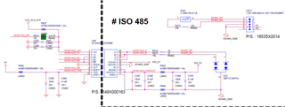
My customer finish their ISOW1432 circuit and start PCB design. Would you please helping to check their layout? Thanks for your kindly help.

Best regards,

Gary Teng

link_M201.zip

  • Hi Gary,

    Thank you for sharing the schematic and PCB layout, please allow me to review them and come back to you tomorrow.


    Regards,
    Koteshwar Rao

  • Hi Gary,

    Apologies for the delay in response and thank you for your patience. Please find my review comments below,

    1. Schematic
      1. The selected ferrite bead (FB) part number ACMS100505A600 only offers 60Ω impedance, please consider a different FB which offers >300Ω impedance from 30MHz to 1GHz. You can also use the one from ISOW1432DFMEVM.
      2. We recommend that you keep GND1/GNDIO node separate from system GND on the primary side. Please refer to ISOW1432DFMEVM or ISOW7741DFMEVM for example.
      3. Otherwise, everything else looks good.
    2. PCB Layout
      1. The decoupling capacitors and FBs on VISOOUT/GND2 are currently located beneath device on a different PCB layer. For best emissions performance, we recommend that nothing is run underneath the device and avoid any noise coupling.
      2. Once GND1/GNDIO and system GND are separated on the primary side, the I believe the PCB layout is going to be updated accordingly.
      3. Other than this, I didn't see any other major concerns. Thanks.


    Regards,
    Koteshwar Rao