This thread has been locked.

If you have a related question, please click the "Ask a related question" button in the top right corner. The newly created question will be automatically linked to this question.

SN6505A-Q1: Using "Half-Wave Rectifier Without Centered Ground and Center-Tapped Secondary" configuration

Part Number: SN6505A-Q1
Other Parts Discussed in Thread: SN6501, SN6505A

Hi,

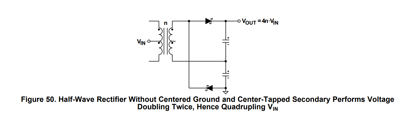
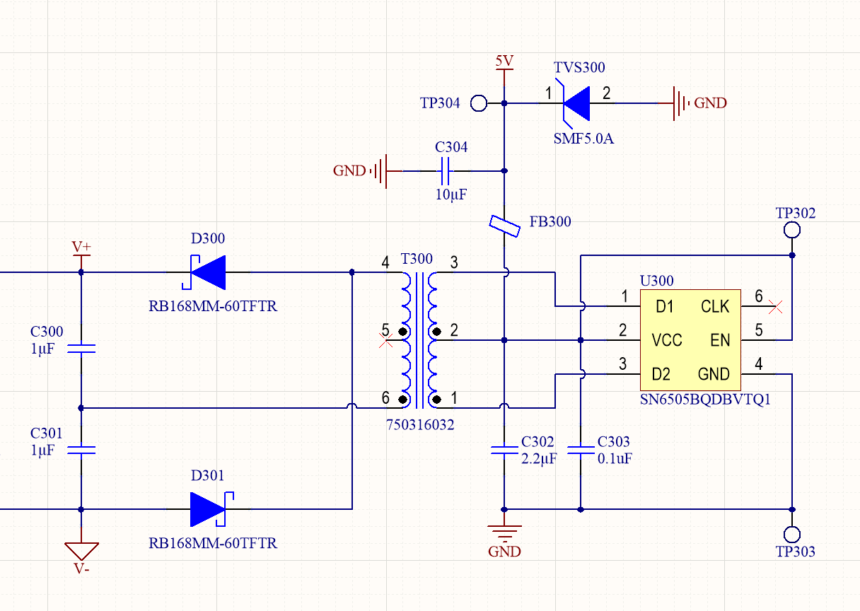
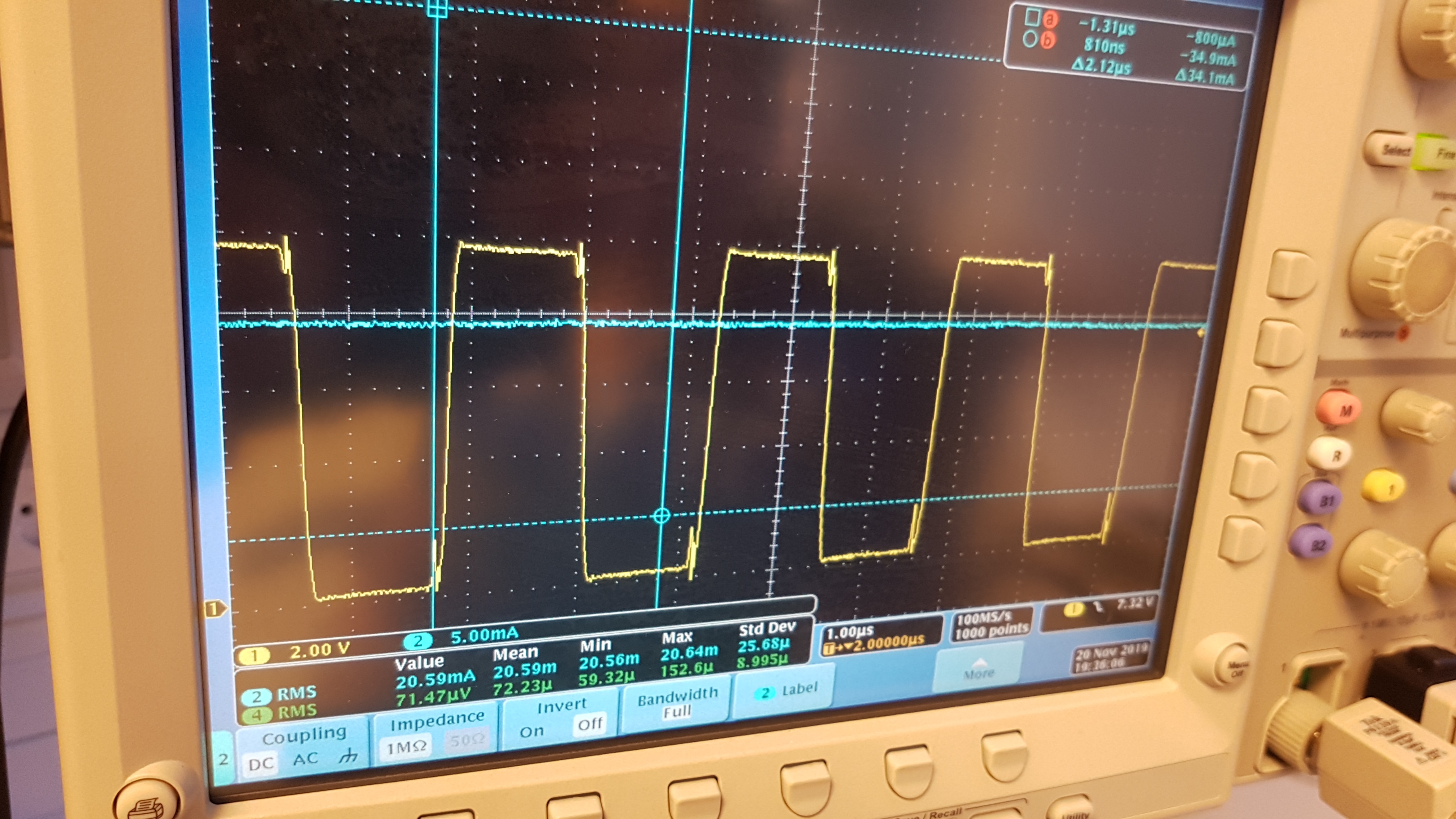
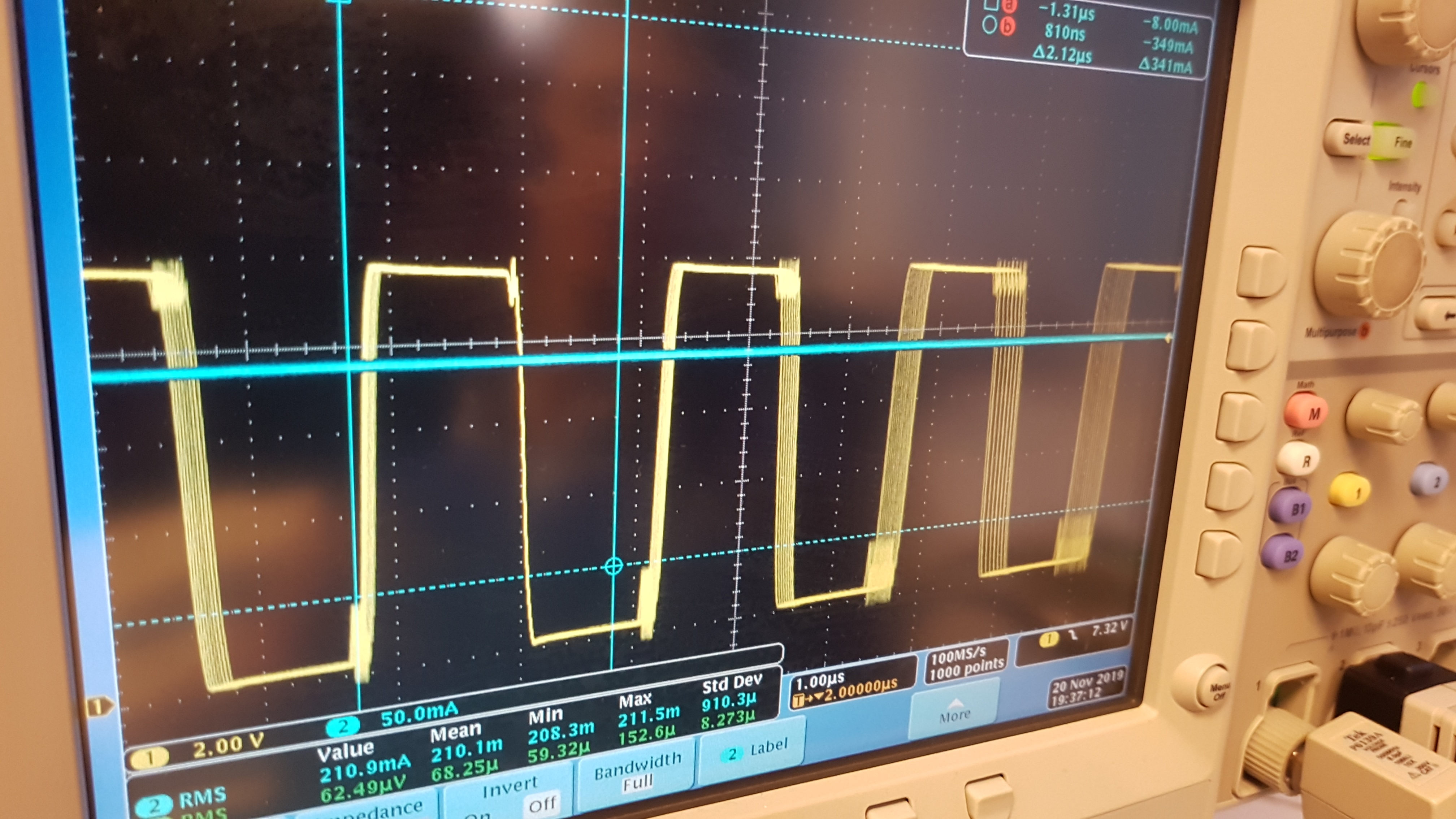
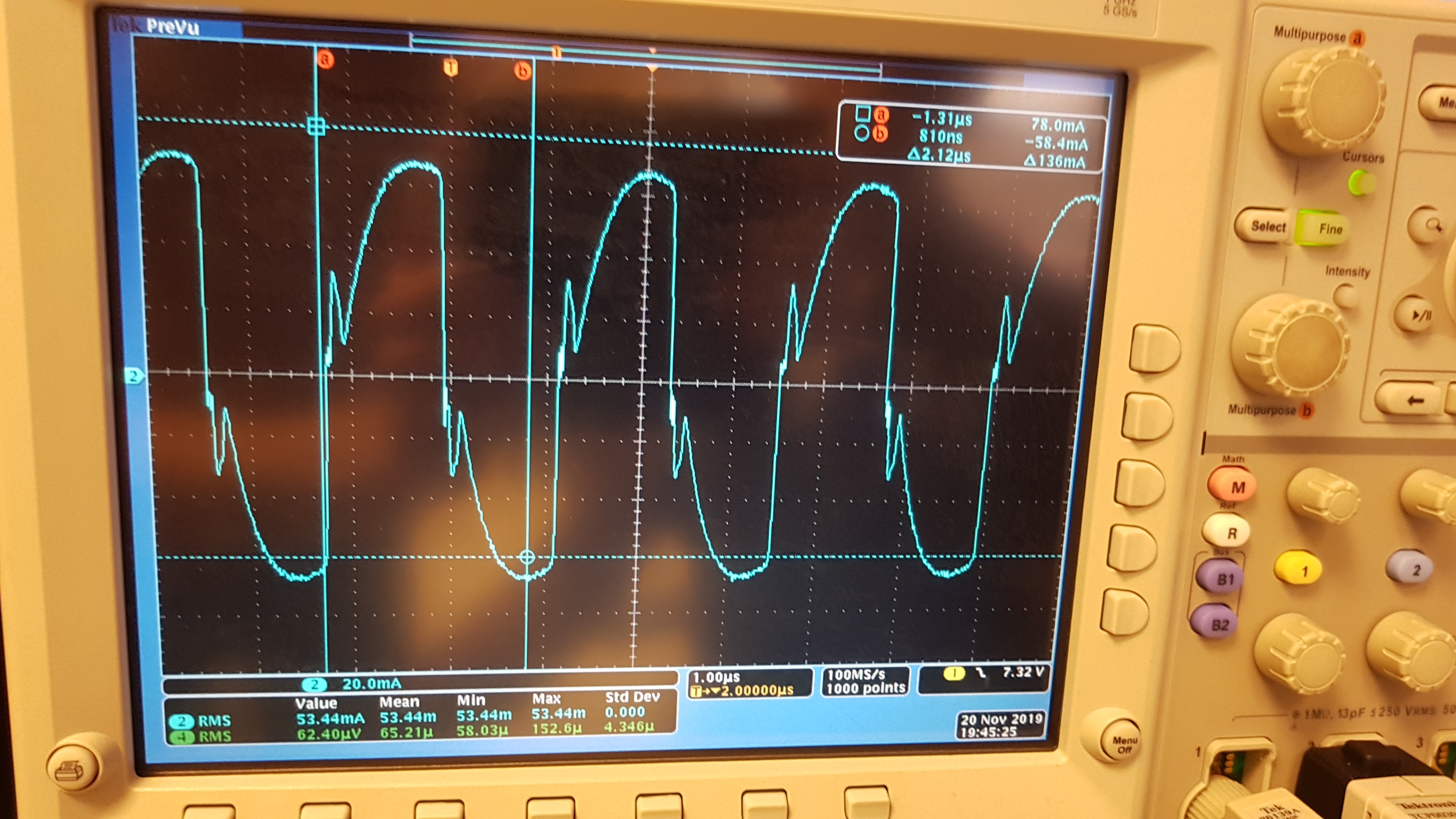
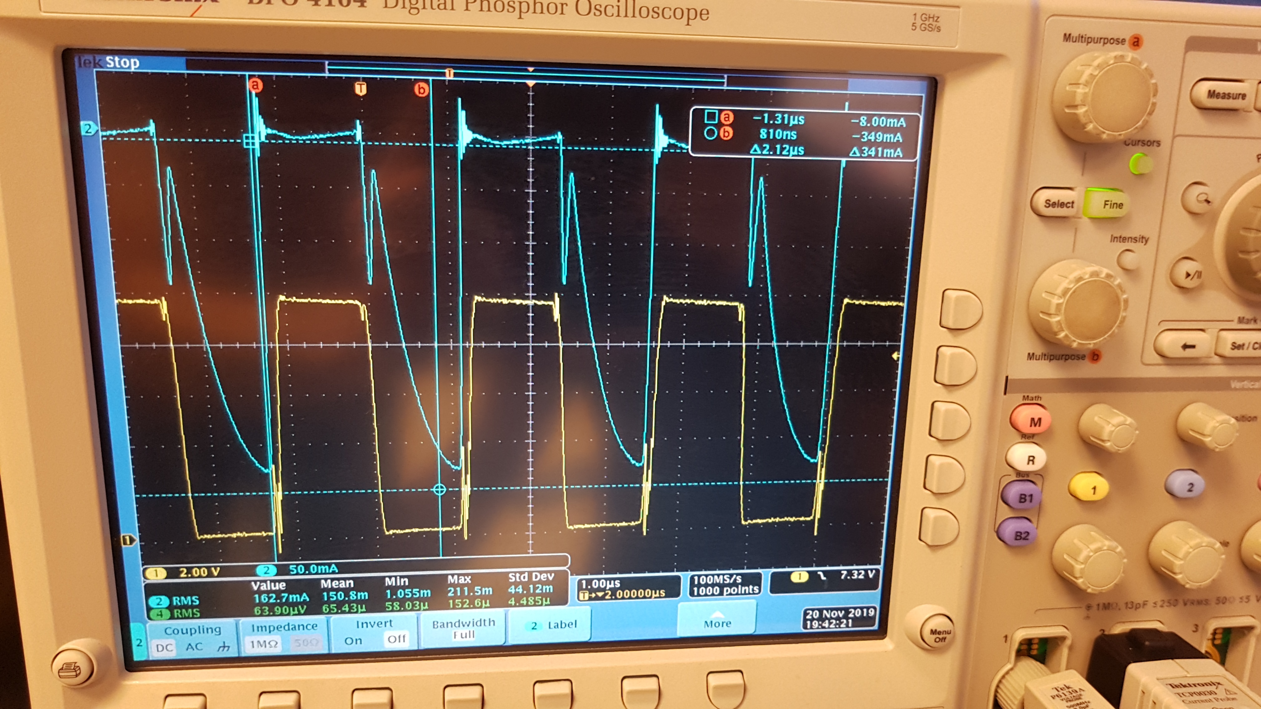
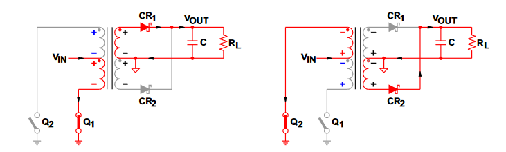
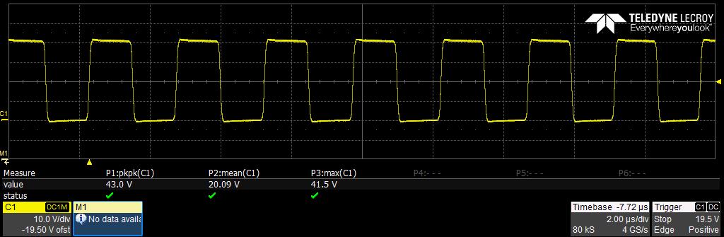
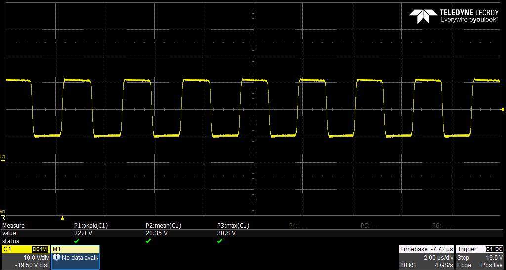
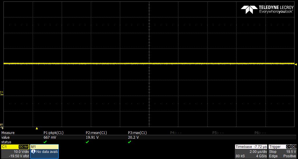
We are in the need of an isolated power supply of around 40V capable of supplying around 5 to 10 mA (we need to supply just one IC high voltage power input). We do not need a regulated power supply as we have some voltage headroom on the isolated power side. We decided to use SN6505A-Q1 with 5V input, 1:2 transformer (WE 750316032: https://katalog.we-online.de/ctm/datasheet/750316032.pdf) and the "Half-Wave Rectifier Without Centered Ground and Center-Tapped Secondary" configuration described in the datasheet as Figure 50. However, when we contacted the transformer manufacturer, they said that this configuration is beyond the specification of the transformer and the SN6505 IC. Nevertheless, we assembled a prototype and it seems to work without a problem (the temp rise is some degrees and the voltage drop is within the specified limits in the datasheet, D1 and D2 experience a maximum voltage spike of 12.5 V according to oscilloscope graph). That being said, we would like to get some insight why such configuration should not be used (at least from the IC side) or what are the potential failures when using it. I have attached the schematic of our design as well as the example from the datasheet.

  • Hi Siim,

    Thank you for posting to E2E! I’m glad to read this voltage-quadrupling configuration is working well.

    Since voltage is multiplied, load current reflected on the primary side will fluctuate to maintain a relationship of transformer Pin ~= Pout. Above a certain voltage, which is not always specified, the transformer could saturate due to insufficient V-t product or parasitic values, collapsing the isolated power supply.

    Potential failures from exceeding voltage ratings will vary from transformer to transformer, but a concern for the SN6505 is current runaway. This can be evaluated by measuring current on the transformer primary side during normal operation and comparing it with the output load current. Please feel free to capture these measurements, and I will provide a follow-up during business hours on Monday.

    Have a great weekend!

    Manuel Chavez

  • Thanks for the quick answer!

    We will get to current measurement ASAP, do you need the waveform of the current or just plain RMS values? From the datasheet, the V-t product seems to be only affected by the primary side voltage and switching frequency. Based on that, we chose a transformer with 20 Vμs V-t product. From your and the transformer mfg comments I understand that this is not the case for our output configuration. Could you provide some sort of reference how to calculate the needed V-t for this output configuration?

  • Hi Siim,

    You're welcome! I'm glad to help. If possible, please do share the current waveform, but a DC measurement of current into the SN6505A-Q1 Vcc pin + Transformer primary side center tap over a sweep of DC load current from 0mA - 20mA should be enough to analyze.

    I apologize for confusion about my V-t product comment. In choosing a transformer compatible with SN6501 or SN6505, V-t product calculation is correct as stated in the datasheet and in the equation you shared above. Certain capabilities of transformers (like maximum output voltage or current) are not always specified, and there may not be an equation to calculate them when transformers are used in voltage-doubling or quadrupling topologies. I meant that even though V-t product is okay from the SN6505 point of view, the higher voltage output might be above what a transformer can handle. These parameters vary from transformer to transformer, and to confirm, 20V-us V-t product is sufficient to use with SN6505A at Vcc = 5V.


    Thank you,
    Manuel Chavez

  • So, we did the DC load test, but we did not have electronic load which could sink so small currents (we have several for 50 A +), so we had to resort to resistors, due to that the numbers are a bit funky. We noticed a quite significant quiescent current, about 18 mA. We are not 100% sure that we managed to disconnect all the circuitry on the PCB from the push-pull output, but thermal camera did not show significant heat dissipation anywhere else but the SN6505 and the transformer. They were degree or few degrees above ambient at 0 mA load.

    I in, mA I out, mA V out, V
    18 0 39,2
    27 1 38,9
    35 2 38,9
    43 3 38,8
    50 4 38,7
    55 4,7 38,6
    66 5,9 38,5
    75 7,1 38,4
    81 7,8 38,3
    88 8,7 38,2
    99 9,9 38,1
    120 12,7 37,8
    127 13,5 37,8
    147 16,1 37,5
    156 17,3 37,4
    172 19,2 37,3
    200 23,1 36,9
    259 30,2 36,3
    317 37,5 35,6
    358 42,6 35,2
    441 53 34,2
    470 56,5 33,9
    560 68 32,8

    We also measured the primary and secondary winding current waveform at approx 20 mA output current, as well as output and input waveform.

    Output waveform:

    Input wavefrom:

    Secondary winding:

    Primary winding:

  • Hi Siim,

    The system appears stable and voltage waveforms are as expected. ~20mA on the primary side is expected at 0mA load due to some parasitic transformer inductances.

    Since the output voltage is 40V, voltage on the transformer secondary side will swing from 0V - 80V as mentioned in 8.3.1 Push-Pull Converter section of the SN6505 datasheet and demonstrated in the image below:


    This means the Schottky diodes will have continually block to voltage up to 80V. To keep the system robust, please replace RB168MM-60TFTR diodes with components that can withstand 80V reverse voltage or greater.


    Thank you for sharing this promising data!


    Respectfully,
    Manuel Chavez

  • Hi,

    We measured the output voltages, and did not see any voltages over 40V. I think it is due to the fact that, we have different output configuration and our center tap is not connected. We have no problem with switching to RB168MM100TFCT-ND, but we would just like to understand our system/circuitry.

    From the first circuit schematic, the voltage waveforms for the secondary side transformer pins:

    Pin 4:

    Pin 5:

    Pin 6:

  • Hi Siim,

    That is true. The 2x voltage swing should be from -20V to 20V across the transformer (pin 4 with respect to pin 6) in this topology, so the maximum blocking voltage of the diodes should only be above 20V.

    I apologize for my mix-up! No swings of 80V are expected in this schematic.


    Thank you,
    Manuel Chavez