This thread has been locked.

If you have a related question, please click the "Ask a related question" button in the top right corner. The newly created question will be automatically linked to this question.

SN74LVC1G17-EP Input Overstress

Other Parts Discussed in Thread: SN74LVC1G17

Hi,

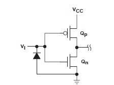
I am performing reliability analysis on a circuit design.  One failure mode is the possibility that the input of the SN74LCV1G17-EP Schmitt Trigger is exposed to greater then 6.5 VDC (the maximum specified rating).  The datasheet does not specify the input topology, but does indicate that there is no clamping diode from input to VCC.  The two over voltage conditions are 15 V current limited by 40kΩ or 7.5 V limited by 10kΩ (375 uA and 750uA respectively).  What are the failure modes of the part in this case, does it get stuck high or stuck low?

I suspect there may be a Zener diode on the input to provide ESD protection.  If the input current is sufficient to overstress this zener, it may fail short and then the output of the device stuck low.  Is this the case?

Is there a failure mode of the input that could cause the device to become stuck high after an overvoltage condition on the input? 

  • Hi Jesse,
    As per the datasheet of SN74LVc1g17 ,there is no ESD between Vcc and input. There will be ESD for all pins to gnd however ,I am unsure about the internal design architecture of it and the diode type .
    The overvoltage application needs to be within the limits specified on the abs max of 6.5V while 15V or 7.5V is way above the abs max .Although you have the current limiting resistor in place to limit the current within the abs max this doesn't guarantee the parts performance over long term .
    The failure mode would be EOS (Electrical overstress) on the pin .The stuck high or stuck low condition is the latch up you are talking about i believe which is defined in the datasheet to exceed 100mA as per JESD78 . I think they perform this under max recommended operating voltage (5.5V ).
  • Jesse,

    I think your question can be answered best by the high reliability team.
  • Jesse, the apps engineer who supports this device is out this week. He will reply to your post when he gets back on Monday.
    Thanks,JV
  • Hi Shreyas,

    This agrees with what I was thinking. I am still unsure if the latch-up with the series current limiting. It all depends on how much current the ESD diode on the input can handle before it fails due to EOS. Hopefully someone in the high reliability team can answer next week when they return.

    Regards,

    Jesse
  • Jesse,

    Unfortunately, we do not characterize or validate the failure modes to conditions beyond absolute max conditions.

    Since there is not an ESD diode to VCC, I would expect an overvoltage to stress gate oxide.

    From SCA010, a simplified input structure is shown page 40.

    I would surmise that this oxide failure could result in the P and/or N channel transistors failing in the stuck on or off as the result.

    Regards,

    Wade