Other Parts Discussed in Thread: SN65LVDS31, SN65LVDS33, SN74LVC2G04, SN74LVC1G79, SN74AUC1G04, SN74HCS74
Good morning,
I have a question regarding calculating the maximum operating frequency for a non clocked device.
A TI rule of thumb says inverse of 2 x tpd or inverse of tPLH + tPHL define the maximum operating frequency.
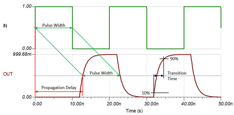
How I see the propagation delay is-> shifts the input signal rising by tPLH and it shifts the signal falling by tPHL.
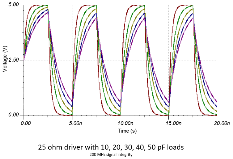
I also think rise time and fall time also takes role on operating frequency. I have couple questions for you to clear my mind and help me understanding the operating frequency calculation and what I expect to see as an output of SN74LVC2T45 with a certain input.
1-) In my application, Vcca is 3V3 and Vccb is 5V. For these voltage levels maximum tPLH->4.4ns and maximum tPHL is 4ns. tPLH + tPHL -> 8.4ns. So maximum operating frquency of this IC is 119 MHz.
What do I expect to see if I have an 80 Mhz clock as an input with 1ns rise and fall time (20-80%). When I check the datasheet of the level shifter Dt/Dv Input transition rise or fall rate is specified as 10ns/V max when VCCi is 3.3V.
Could you please draw me an input clock 80 Mhz with a 1ns rise time (20-80%) to this level shifter and what do I expect to see as an output?
When I look at the datasheet page 12 -> VCCI/2 appears at the output with VCCO/2. I don't understand how this is possible with a 33ns rise time of a 3V3 level signal?
Do you think you could help me here for me to understand the whole concept?
Best regards
Onur


