This thread has been locked.

If you have a related question, please click the "Ask a related question" button in the top right corner. The newly created question will be automatically linked to this question.

SN74LVC2T45: Frequency calculation

Part Number: SN74LVC2T45
Other Parts Discussed in Thread: SN65LVDS31, SN65LVDS33, SN74LVC2G04, SN74LVC1G79, SN74AUC1G04, SN74HCS74

Good morning,

I have a question regarding calculating the maximum operating frequency for a non clocked device. 

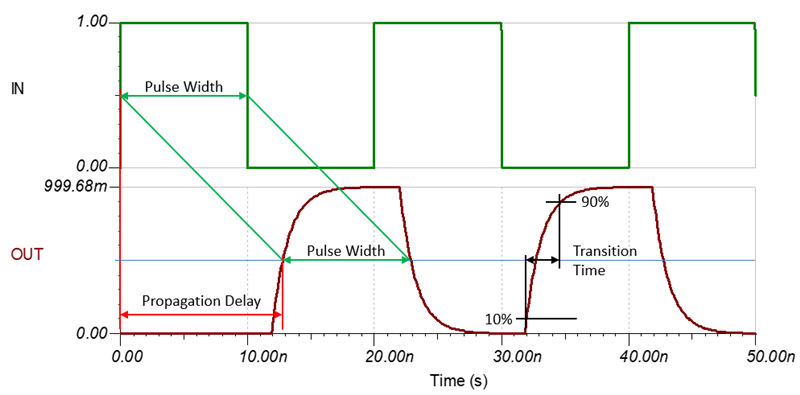
A TI rule of thumb says inverse of 2 x tpd or inverse of tPLH + tPHL define the maximum operating frequency. 

How I see the propagation delay is->  shifts the input signal rising by tPLH and it shifts the signal falling by tPHL. 

I also think rise time and fall time also takes role on operating frequency. I have couple questions for you to clear my mind and help me understanding the operating frequency calculation and what I expect to see as an output of SN74LVC2T45 with a certain input. 

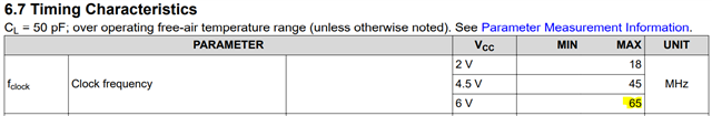
1-) In my application,  Vcca is 3V3 and Vccb is 5V. For these voltage levels maximum tPLH->4.4ns and maximum tPHL is 4ns. tPLH + tPHL -> 8.4ns. So maximum operating frquency of this IC is 119 MHz.

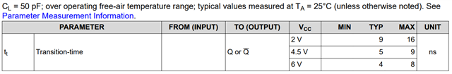
What do I expect to see if I have an 80 Mhz clock as an input with 1ns rise and fall time (20-80%). When I check the datasheet of the level shifter  Dt/Dv Input transition rise or fall rate is specified as 10ns/V max when VCCi is 3.3V. 

Could you please draw me an input clock 80 Mhz with a 1ns rise time (20-80%)  to this level shifter and what do I expect to see as an output? 

When I look at the datasheet page 12 -> VCCI/2 appears at the output with VCCO/2. I don't understand how this is possible with a 33ns rise time of a 3V3 level signal? 

Do you think you could help me here for me to understand the whole concept?

Best regards

Onur

  • The rise time does not really matter for this; the device switches when the input voltage crosses the threshold, which is somewhere between VIL and VIH (typically, it's near VCC/2).

  • Hi Onur,

    Generally speaking, it's best to use a clocked device in the same family to determine the maximum operating frequency of a buffer ([FAQ] What is the maximum data rate (or operating frequency) for a logic gate or buffer?) -- by using this limit, you can be sure that the device will operate properly and not have any concerns with the below discussion. I'm providing the info below just to help you further understand the topic.

    -

    When I check the datasheet of the level shifter  Dt/Dv Input transition rise or fall rate is specified as 10ns/V max when VCCi is 3.3V. 

    This is only in reference to the input transition rate which generally doesn't significantly affect the operating frequency, but the output transition rate has much to do with the maximum frequency of operation -- and it's not provided in most datasheets. This FAQ may help: [FAQ] What is the output transition rate for a logic device?

    The above graphic shows propagation delay (t_PLH) for a typical buffer (ideal input, realistic output). Key points here are that the delay is measured from 50% input to 50% output, even though the device may switch at a different voltage than 50%. Usually this isn't an issue because the input signal transitions very quickly in testing (less than 2.5ns) and the difference in threshold is usually minor.

    The above graphic assumes we're operating at a frequency, voltage, and load condition that is supported by the device.

    By varying the load condition at a set frequency, we can see that the output signal changes significantly. Some of the waveforms shown don't even reach 10% or 90% to provide a measurement point for the transition rate. Also, the device is no longer producing a square wave, but it's still producing a 200 MHz signal.

  • Good morning,

    Part-1

    Thanks for the information, I have 5 components in my circuitry. First one is FPGA generates 3V3 switching signal. 

    Second and third components are LVDS Driver(sn65lvds31) and LVDS receiver(sn65lvds33) 

    Third and fourth devices are level shifter 3V3-5V(sn74lvc2t45) and an inverter (SN74LVC2G04)

    If I understand you correctly, I need to find same family where a clock rate is mentioned and for inverter SN74LVC2G04 -> it is SN74LVC1G79(160MHz)

    Do you think you could help me to find other part numbers with the same family members where I can see maximum operating frequency? 

    Note:For SN65LVDS31 in the datasheet, Figure 7-1 shows current vs frequency graph where the frequency goes up to 200 Mhz. 

    Part-2

    I think you explained the propagation delay, rise/fall time clearly but I am not 100% sure if I correlate them correctly. 

    Propagation delay-> where the input voltage level crosses the threshold(VCCA/2) in tPLH or tPHL duration we see the output at (VCCB/2). 

    And you mentioned output transition rate which I see this as a rise or fall time of the output which changes due to the load. If this transition time is too long, even though the signal switches with the expected frequency, I cant see this signal reaches the desired voltage levels.

    In the datasheet, may I find this transition rate information with different loads and with different voltage levels?

    Thanks a lot for the good information and thanks again or the help in advance.

    Best regards

    Onur

  • Hi Onur,

    I expect that 160 MHz is a pretty accurate maximum frequency for the LVC family of logic. You won't find an inverter that includes the maximum clock frequency because it doesn't include a clock input. That's only specified for devices with clock inputs (ie internal flip-flops).

    I'm a bit confused as to why you are converting the voltages from 3.3V to 5V. The SN65LVDS31 supports a 3.3V input voltage:

    As for a 3.3V inverter that supports 200 MHz, I'm afraid I don't have one of those. If you can step down to 2.5V, then you could use the AUC logic family (SN74AUC1G04) which supports up to 275 MHz at 2.5V. It also allows for 3.3V inputs when the supply is 2.5V, and the output would still meet the requirement of the SN65LVDS31.

    I think you explained the propagation delay, rise/fall time clearly but I am not 100% sure if I correlate them correctly. 

    There isn't really a correlation between propagation delay and maximum frequency. A "rule of thumb" that many engineers use is f_max = 1/(2*tpd) -- but a rule of thumb is just there to give you an idea of operation, and not to set any hard limit. Really the best way to determine maximum frequency is to put the device in the conditions that you expect to be operating and test it yourself.

    Technically, you can have a huge propagation delay in a circuit while still maintaining the original input frequency. For example, if I were to line up 100 inverters with 2ns of delay each and input a signal, the output would have 200ns of delay, but it would be able to accurately reproduce any signal that the inverters can support.

    And you mentioned output transition rate which I see this as a rise or fall time of the output which changes due to the load. If this transition time is too long, even though the signal switches with the expected frequency, I cant see this signal reaches the desired voltage levels.

    In the datasheet, may I find this transition rate information with different loads and with different voltage levels?

    I also included an FAQ that explains how to determine this for a device, although it's not perfect. Some devices have it characterized -- most do not.

    For example, the SN74HCS74 includes the output transition time:

    Using these values, we can try to calculate the maximum operating frequency:

    f_max = 1/(2*t_t) = 55.55 MHz

    The datasheet also includes the maximum operating frequency:

    As you can see -- these two don't quite line up, but they are fairly close.

    -

    The best advice I can give you is to get some parts and test them in a similar setup to what you plan to use in your final system.

  • Good morning,

    Thanks a lot again for all information. Let me summarize my application again. 

    FPGA ---3V3 signal--> LVDS Driver(sn65lvds31) ---LVDS--> LVDS Receiver(sn65lvds33) ---3V0 signal--> Level shifter(sn74lvc2t45)--5V signal--> Inverter(SN74LVC2G04)---5V Inverted Signal---> IC(Expects 5V Input)

    Above info explains why I have to shift the voltage level to 5V. 

    I see you explained frequency info for SN74HCS74 but I don't have this IC in my circuitry. I have SN74LVC2G04 instead which is a dual inverter with a  maximum tpd of 3.2ns at 85 degrees. Rule of thumb 1/(2*tpd) says-> 156.25MHz. And it is also a SN74LVC device which in theory, I am supposed to expect 160 MHz operating frequency? 

    I will check one bye one the signal shape, output rise and fall times and propagation delay for each IC in my circuitry. 

    Thank you in advance for your help

    Best regards

    Onur Kusakoglu

  • You do not need the inverter if you exchange the two LVDS signals.

    What is that receiving IC? Might it have TTL-compatible inputs?

  • The reason why I have the inverter is the active failsafe which assures a high level output with no input. In my application, I shouldn't see any high unless I drive it high. So I send and inverted signal from FPGA and invert it again to prevent a high signal(during fail safe) reaches to my end point.

  • Hi Emrys,

    Datasheet information gives the tpd time or tphl and tplh times with minimum and maximums. Shall I consider these ranges as distortion times?

    For example in same IC in same conditions, Is this number constant? or it really deviates in between minimum and maximum ranges?

  • Hi Onur,

    Propagation delay is given for a particular voltage range and temperature range. Typically it will be the largest (worst) at the lowest voltage in the range and the highest temperature. You should expect the value of delay to be consistent at a single operating condition (for example, 3.31V at 25C). Note that high speed operation with a heavy load will heat the device, which will impact performance.

    Additionally, there can be variations in timing from one device to another, commonly called "process variations".

    We can only guarantee the limits in the datasheet, so I would recommend designing with those. The maximum value is generally of the most concern -- quite often the minimum is not listed or is put at a generic value (for example, 1.5ns).