This thread has been locked.

If you have a related question, please click the "Ask a related question" button in the top right corner. The newly created question will be automatically linked to this question.

SN74HCS594-Q1: LED flashing when doing the BCI test

Part Number: SN74HCS594-Q1


Hi team,

My customer has encountered an issue about the LED flashing when doing the BCI test.

Issue description:

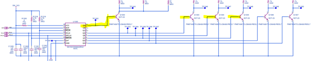
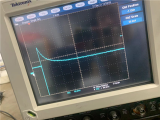
Customer loaded the data into the SN74HCS594-Q1, (all output set to 1), during BCI test we do not modify any data and we see the LED flashing within the range of 110Mhz~200Mhz on different channels (which means some LED still on and some LED channels off). We test 2 boards and both of them happen the issue. We provide all the 1 (high voltage level ) to the input, here is the schematic:

LED driver.pdf

You could see the video below to check the issue phenomenon:

Could you please kindly help to review the customer schematic design by today since they are under EMC test process, if you have any idea of debug this issue, please also provide to us since it is urgent, thank you.

  • All outputs will go low if there is a falling edge on /RCLR, or a falling edge on /SRCLR followed by a rising edge on RCLK. It's possible that R1318 and R1319 can pick up noise.

    Or the power supply could be affected.

    Which signal(s) do you inject current into?

    To recover from wrong data, regularly shift in the correct data.

  • Hi Ladisch,

    Sorry for not quite sure about the BCI test. What do you mean by the following sentences? Or what should I ask to customer? 

    Which signal(s) do you inject current into?

    Besides that, the phenomenon is that different channels have different performance. (Some channel output 0 and some channel output 1, so you could see in the video the LED is flashing). What is the suggestion of R1318 and R1319 and what is the review result of the customer design? Is that OK or any component value should be modified? Thank you! 

  • Is the target of the BCI test some communication line (i.e., the inputs of the shift register), or something else?

    I would suggest to replace R1318/9 with 0 Ω, but then the register would not be reset at power up.

    If the outputs of a single chip have different values, then SER and SRCLK are affected. The only way to recover from this is to shift in new data.

    The schematic does not show how the input signals are driven. Protecting these signals probably involves changes there, and to the board design.

  • Hi Ladisch,

    Sure so you suggestion is modify the R1318/9 to be 0 ohm to have a try right? But I think these are pull up function resistors so why should we remove them and if we remove the resistors the 3.3V will directly connected to the SRCLR and RCLR. We are afraid this connection will damage to the chip. 

    If the outputs of a single chip have different values,

    Yes from the phenomenon we see the LEDs flashing randomly and initially we use software method to set all the 3 chips output as 1. But in BCI test we may not be able to test the CLK and other signal. We just provide the power supply and to see what will happen with LEDs in the BCI test. We would like you to review the chip peripheral circuit and provide some suggestions for customer to pass the BCI test within the range of 400Mhz.

    If the SER and SRCLK are affected, how could I modify the schematic or add some circuit to resist this interference? What else information do you need so I would reach out to customer to get them, thank you.

  • CMOS inputs have high impedance and can be connected directly to VCC. (A possible problem here is that the RC combination was intended to generate a low pulse at power up.)

    The question is how the noise does get to the inputs. Where exactly does it enter the device, and how does it go from there to the shift register?

    In general, to protect against high-frequency noise, add some kind of low-pass filters. What is the frequency of the normal input signals?

  • Hi Zirui,

    The first issue I see in the schematic is that there are no current limiting resistors on the bases for any of the control transistors:

    This will result in essentially a short to ground condition for the SN74HCS594-Q1 any time an output is in the HIGH state, and it may permanently be damaged by this.

  • Hi Maier,

    Customer has used the transistors who integrates resistors into it, we would like to know that what input should we add low pass filter?  Data or clock input? Thank you.

  • You need LPFs on every trace that is affected by the noise. When in doubt, all three of them.

    A different board layout might be able to shield these traces better.

  • Hi Ladisch,

    Do you need to review the customer SN74HCS594Q1 part layout? Therefore do you suspect it is an issue related to layout and noise? Thank you.

  • It might be possible to improve the layout with a larger distance between the trace and the noise source, or by adding ground traces in between. But I do not know what the space constraints on the board layout are, so this might not be helpful. See, for example, the ESD Layout Guide.

  • Hi Ladisch,

    I collected customer's one of the SN74HCS594-Q1 layout, please kindly refer to the screen shot, if anything need to improve, please let us know, thank you!

  • Can you show the entire path that the SER/RCLK/SRCLK signals take? Where do they originate?

  • Hi Ladisch,

    Update the test results:

    Customer added 50ohms resistor on every trace: SER, RCLK, SRCLK and then the BCI test passed. Now the new issue is:

    When they did ESD test and measured the waveform and found that the SER signal has been hit high and low by the ESD. Do you have some suggestions on customer's ESD test of  customer's current schematic design? Thank you!

  • It might be possible to improve the layout with a larger distance between the SER trace and the noise source, or by adding ground traces in between.

    Can you show the entire path that the SER signals takes? Where does it originate?

  • Hi Ladisch,

    Here is the layout information:

    Is there any improvement of the layout for ESD test? Thank you.

  • And where is SER?

  • Hi Ladisch,

    Here I collected customer layout again and could you please kindly help to review it with the schematic I previously sent to you? Thank you!

    Besides, below is the phenomenon video:

    Could you please help to provide some suggestions on their layout to improve the ESD performance? Thank you very much!

  • Pin "14L" just goes to a via; i cannot see the entire trace.

  • Hi Ladisch,

    Update some addition information, Pin 14 is SER, Pin 12 is RCLK, Pin 11 is SRCLK. Customer made the following countermeasures on SER pin:
    1. String a 50 ohm resistor on the signal line (tried close to the MCU and close to the LED driver)
    2. Add a capacitance to ground with 10nF and a withstand voltage of 50V.
    3. Add a pull-up resistor of 4.7K/9.4K, and a 10nF capacitor in parallel with the pull-up resistor (want to absorb pulses).
    None of the above measures are effective. Customer also  used an oscilloscope to capture the ESD graph as follows:

    With these information and schematic & layout above, could you please kindly help to provide us some suggestions with ESD issue? Thank you!

  • I cannot see where on the board the noise is coupled into the SER trace. (That would be the best place for countermeasures.)