This thread has been locked.

If you have a related question, please click the "Ask a related question" button in the top right corner. The newly created question will be automatically linked to this question.

SN74LVC08A: Input leakage current at Vcc=0V

Part Number: SN74LVC08A

Hi support team.

I have asked a question from my customer regarding input leakage current at Vcc=0V, Ta=-25℃.

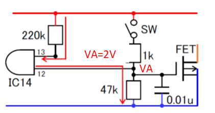
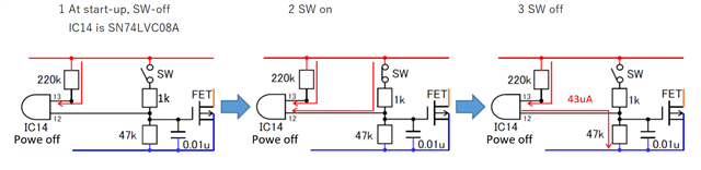
My customer made sure the large leakage current (about 43uA) under using pulled-up with 220K and pulled down with 47K at Vcc=0V, Ta=-25℃.

Is this result correct?

Please refer to the following figure.

I can find the input current specification at Vcc=3.6V but not under any other condition.

Could you please provide the specification regarding a input leak current at VCC=0V?

Best regards,

Higa

  • The input leakage current would be pretty much independent from the supply voltage.

    A current of 43 µA through a 200 kΩ resistor would result in a voltage drop of 9.46 V. Where does this voltage come from?

  • Hi Ladisch-san

    Thank you for your reply.

    The current of 43uA is not from 200k, but the leakage current (source current) from the 12-pin input of the SN74LVC08A.

    The current flowing through 200k is unknown.

    It was also found that the other inputs 1 and 4 were pulled up to the 5V lane with a 10kΩ resistor.

    Best regards,

    Higa

  • A damaged input might leak current; this would probably be caused by overvoltage. But when VCC is 0 V, where does this current come from? Is there a voltage drop over any of the pull-up resistors?

    How exactly is the current being measured? Might it be leakage from the FET?

  • Hi Ladisch-san

    There was a part of the individual customer's report that was lacking in explanation.
    They confirmed that the midpoint voltage (VA) of 47K and 1K was 2V. (Please refer to the figure below.)

    I also thought the input was damaged and asked my customer to disconnect the input (pin 12) and isolate if the leak current was the cause.
    The result was a leak current from the device's input as the VA voltage was 0V.
    However, I do not understand why such a large leakage current is generated in the situation of VCC = 0V.

    Do you still think the device is damaged?

    Best regards,

    Higa

  • CMOS inputs have a high impedance. A current of 43 µA implies damage.

    But please check that there is no leakage through the FET.

  • Ladisch-san

    Thank you for your kind support.

    My customer confirmed that there was no leakage current from the FET by disconnecting the input (pin 12) and the FET gate so that no voltage appeared on the 47kΩ resistor (nearly 0V).

    However, my customer noticed that the information to me was incorrect and reported a correction.

    I told you that VCC = 0V, but it was wrong and VCC = 5V.

    In the data sheet, VCC has a maximum of 3.6V, which is not a recommended condition.

    Is it possible to increase the leak from the input port?

    Best regards,

    Higa

  • The electrical characteristics are guaranteed only when the recommended operating conditions are met.

    What is the voltage when pin 12 is disconnected but with the resistor still connected to the FET gate?

  • Hi Ladisch-san

    Thank you for your reply.

    It is nearly 0V at the FET gate.

    Regards,

    Higa

  • So the leakage current definitely comes out of pin 12.

    Then I can only repeat what I said earlier: the device is damaged, probably due to overvoltage/ESD.

  • Ladisch-san

    Thank you for answering.

    I apologize my late response. 

    Is it correct to understand that an abnormal leakage current does not occur when used with VCC=5V? 

    Best regards,

    Higa

  • A 5 V supply is outside the recommended operating conditions, but LVC is designed to withstand 5 V. And high leakage currents should happen only at high temperatures. 43 µA is much beyond any normal leakage.

  • Hi Ladisch-san

    Thank you for your support.

    I understand.

    This issue has solved.

    Thanks!

    Higa