This thread has been locked.

If you have a related question, please click the "Ask a related question" button in the top right corner. The newly created question will be automatically linked to this question.

LSF0108: Some design question for LSF0108

Part Number: LSF0108
Other Parts Discussed in Thread: SN74AXC8T245

Dear SIrs,

My customer has some questions that need your help!

The questions as below.

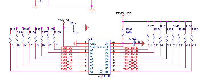
1.  As below design, remove pull high resistors of A and B side, and short R195.

 In such configuration, in the datasheet 6.6 Electrical Characteristics state, there is 30ohm Ron for each channel.

checked A/B side waveform, both of them are 1.2V clock waveforms.

May I think it is the bypass mode of LSF0108? 

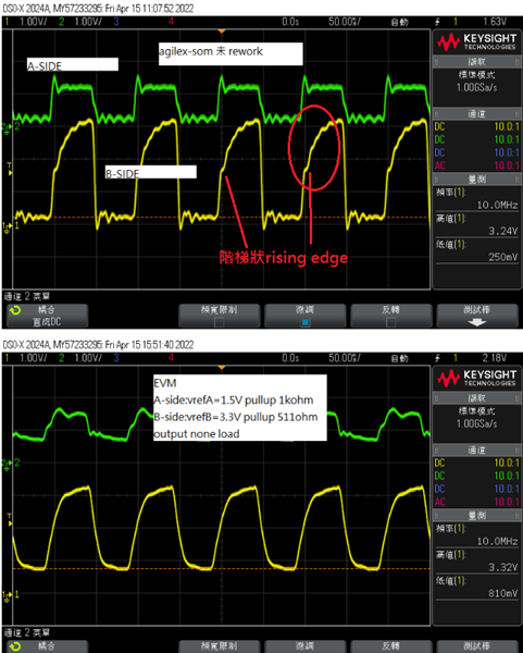
2. in another test circuit for 1.2V to 3.3V, and measure the A/B side waveform as below and found B side have ladder rising edge waveform on customer board.

Such waveform will cause wrong data output in customer system.

After modified LSF0108 EVM with the same setting of customer board, there is no such rising edge waveform in B side.

May I have your comments that is there any way to improve the issue on customer board.

Thanks.

  • The LSF is a passive switch. The pass transistors are closed only when an external device drives a low-level signal. For a high-level signal, the switch is open, and the output voltage is determined only by the pull-up resistor. See [FAQ] How do the LSF translators work?

    1. R195 limits the current flowing into Vref_B and out of Vref_A. Do not short it.

    2. That ringing on the signal lines could be caused by long traces/cables.

    Anyway, are the signals bidirectional or unidirectional? In the latter case, a buffered translator like the SN74AXC8T245 would be a better solution.