Hi team,
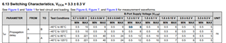
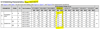
In the SN74AXC4T774QPWRQ1 data sheet, 6.13 states "Switching Characteristics, VCCA = 3.3 +/- 0.3V",
in the table above, "tpd" when "B-Port Supply Voltage (VCCB)" is "1.2 +/-0.1V" is indicated as "min.0.5ns, MAX.8ns".
Could you tell us about this delay time and provide us with the following ① to ⑤?
By the way, a-Port 3.3V and B-Port 1.2V signals with a period of 25 MHz output from a-Port to B-Port is my customer's target.
They are trying to examine how much duty will collapse due to the difference between the rise delay time and the fall delay time.
① They imagined that "min.0.5ns, MAX.8ns" would vary depending on the temperature, is it correct? Is there any other factor that effects this?
②If the temperature is constant (assuming 25℃), is it correct to assume that the rise delay time and fall delay time are the same?
③If the delay times are different, how many ns will the rise delay time and the fall delay time be respectively?
④Could you tell us the rise delay time and fall delay time at "-20°C", "25°C", "55°C", "70°C".?
⑤ If you have a characteristic graph that shows the relationship between temperature and rise fall delay time, could you provide it?
Regards,
Ohashi