This thread has been locked.
If you have a related question, please click the "Ask a related question" button in the top right corner. The newly created question will be automatically linked to this question.
Dear TI Support Team,
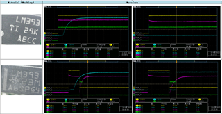
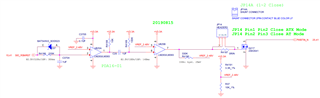
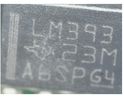
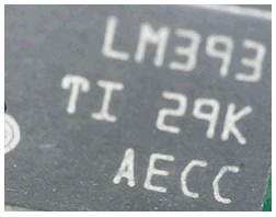
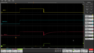
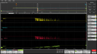
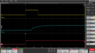
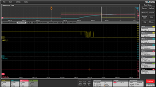
The LM393DR IC has two different marks. It seems that there is a difference between good and suspicious units. Please try to check the ccompare waveforms of the good and failed unit. Can you please help to clarify why does LM393DR IC has two different marks and performance?
Compare waveform:
There are six manufacturing sites for the LM393DR; different marking styles are expected.
Please show the schematic.
Hi Hins,
Thanks for your post. It would be helpful if you could share your schematic as well as let us know which waveforms corresponds to which pins.
This device is also undergoing PCN so you may be getting a mix of the old and new die right now. Please see section 2.2 - 2.4 of this app note for more information about the differences: Application Design Guidelines for LM339, LM393, TL331 Family Comparators (Rev. C)
Attached please find the shematic for your reference.
Currently, we haven't received any PCN documents. Can you please help to clarify the difference between the old and new die?
The mark is displayed as "LM393 23M ABSPG4" (Old Part), as shown in the figure below, which is usually normal.
However, the mark of the faulty part is displayed as "LM393 TI 29K AECC"(New Part), and the symptom are similar to the previous waveforms.
The LM393 does not have rail-to-rail inputs; it needs a headroom of 2 V to the positive supply. With a 3.3 V supply, you should not use input voltages above 1.3 V.
The LM393LV would have rail-to-rail inputs.
Hins,
The differences between the old and new die is stated in section 2.2 - 2.4 of the app note that I linked: Application Design Guidelines for LM339, LM393, TL331 Family Comparators (Rev. C) How to identify them is also mentioned. To determine which die is used, look at the Chip Country of Origin (21L) field on the box or bag packing label. If the Chip Country of Origin (21L) CCO: field says USA, then this is the classic die. If the Chip Country of Origin (21L) CCO: field says CHN, then this is the new die.
It looks like your inputs are violating the common mode range. For the new die, the output will toggle high when the inputs are both out of the range. For the old die, the output will toggle low. I would either divide the inputs down to be within the range or use LM393LV, which was designed for this exact use case and is a drop in replacement.
Yes. Based on this current circuit, I tried to use a rail-to-rail component similar to LM393LV. i.e. LM393LVDR is used instead of LM393 directly, but found the noise in the comparison, the related waveform for your reference.
For slow input signals, you need hysteresis. (This is also true for the LM393; you were just lucky so far.)
Hello Hins,
It does look like chatter so you may need to add some more hysteresis. What does the input on pin 2 look like as it traverses through the threshold? Can you also tell me about the purpose of this circuit?
It used this comparator to set the function of analog automatic power-on.
If remove C20, measure the comparator Pin 1,2,3, the waveform as following. But adding more delay still can not fix this issue.
Hysteresis: https://www.ti.com/lit/an/sboa219a/sboa219a.pdf?ts=1683790934285
You need hysteresis at the first comparator, i.e., feedback between pins 1 and 3.
Hi Hens,
How much hysteresis did you add? The signal on pin 2 looks to be very slow so as it passes through the reference, any little noise can create that chatter on the output so I would just add more hysteresis. What happens if you put a faster edge signal on pin 2? Do you still see the same issue?
Closing this post as we have not heard from you in a while. Feel free to reply back if you have any more questions.