
- Ask a related questionWhat is a related question?A related question is a question created from another question. When the related question is created, it will be automatically linked to the original question.
Hello all,
this is the circuit where i have a problem:
/cfs-file/__key/communityserver-discussions-components-files/151/CircuitDiagramQuestionTI.pdf
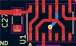
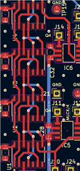
The clock is generated by the component: ECS-TXO-3225MV-122.8-TR This is fed into the SN74LVC74A. This is done so many times in total that the clock is reduced from 12.288 Mhz to 3.072 MHz and to 48 KHz after the fourth element. Soldered the prototype and then I noticed the following problem. It looks to me like the individual control signals are coupling into the supply voltage. If a load is addressed at 3.072 MHz, the supply voltage worsens. After now several days of testing, I was able to narrow down the source of the error to the SN74LVC74A. Also I have three different capacitors (22pF, 100nF, 1uF) instead of 100nF at the respective components placed. Unfortunately without success.
My question: Is the circuit for the SN74LVC74A correct? And additionally, how can I prevent the edge phenomenon "ringing" at the device. This seems to me also as a possible source of error.
Measurements:
Clock generated by the ECS-TX0-3225MV-122.8-TR
Output of the first SN74LVC
Output of the corresponding NB3N551DR2G
Power Supply 3V3 after i connect one probe to the output of the NB3N551DR2G and one probe to the Power supply
power Supply 3V3 when i only connect the probe to the power supply
power supply 3v3 when i have a load on 3MHz and 48Khz
Blue: Near the SN74LVC
Yellow: at the Power Supply
Oscilloscope: UNI-T UTD2052CEX
Probes: Sensepeek 2x SP100
Many thanks for your help in advance


