This thread has been locked.

If you have a related question, please click the "Ask a related question" button in the top right corner. The newly created question will be automatically linked to this question.

SN74LV4046A: Output of PC2_OUT and PCP_OUT

Part Number: SN74LV4046A
Other Parts Discussed in Thread: CD4046B, CD74HC4046A

Hi Team,

I have questions about output of PC2_OUT and PCP_OUT.
Attached is the waveform(only PC2_OUT) from the customer system.
I think that these outputs of T0 to T1 and T1 to T2 are correct, but I think that T2 to T3 is not correct.
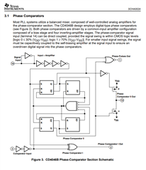
Here, I think PC2_OUT should be "High impedance" and PCP_OUT should be "High" because SIG_IN and COMP_IN are in the same phase.
However, these outputs remain in pre-state(PC2_OUT is High, PCP_OUT is Low).

Is there anything that you think might be the cause?

My understanding about output of PC2_OUT and PCP_OUT is as follows.
Please let me know if this understanding is wrong.
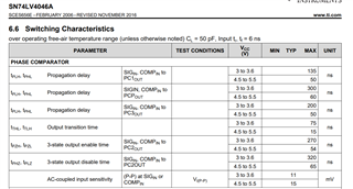
<PC2_OUT>
- This pin is 3-states output.
- A higher frequency at SIG_IN will cause the output to be driven "High".
- A higher frequency at COMP_IN will cause the output to be driven "Low".
- In between these states the output will be in "High impedance".

<PCP_OUT>
- This pin is 2-states output.
- When one of the frequencies of SIG_IN and COMP_IN is higher, it will cause the output to be driven "Low".
- In the other cases, it will cause the output to be driven "High".

Best Regards,

SN74LV4046A_SIGIN_COMPIN_PC2OUT.pdf

  • Hi Atsushi, 

    Phase comparator 2 is a positive edge-triggered flip flop, and from section 7.3 of the datasheet "The circuit functions as an up-down counter where SIG_IN causes an up-count and COMP_IN causes a down-count". In this case I think the output between T2 and T3 makes sense since the output is in a "High" state, sees a positive edge on COMP_IN which causes a down-count to high impedance state, but then sees another high transition on SIG_IN which causes it to increment back to a high state again. Since the width between these edges is only 10 ns this probably can't be seen on the output since it's much less than both the output transition time and propagation delay. The reason why there's brief transitions on the output between T1' and T2' is most likely because the high-Z -> low transition is faster than the high -> high-Z transition, which is confirmed by the specs on the datasheet:

    SN74LV404A is pin-to-pin compatible with CD4046B so the phase comparator and PCP_OUT behavior should be similar. It looks like the CD4046B datasheet has a better diagram showing the details of the phase comparator circuitry:

    PCP_OUT has similar logic to phase comparator 1 and is acting as an XOR gate, except it is pulled low when SIG_IN and COMP_IN are out of phase. Note that PC2_OUT and PCP_OUT are determined by the alignment of the edges of the inputs and not necessarily by their frequency. Let me know if this answers your questions. 

    Regards, 

    Connor 

  • Hi,

    Thank you for your reply.
    The following post says this device design is the same as CD74HC4046A at first reply.
    CD74HC4046A and CD4046B have different schematic.
    Which information is correct?

    SN74LV4046A: SN74LV4046A - Logic forum - Logic - TI E2E support forums

  • Hi Atsushi, 

    Sorry for the confusion, the SN74LV4046A phase comparator 2 is actually more similar to CD74HC4046A since they both consist of 2 D flip flops.

    I believe both schematics have the same behavior, but the implementation might be slightly different. In either case, a rising edge on SIG_IN will increment the output state (i.e. low -> high-Z or high-Z -> high), and a rising edge on COMP_IN will decrement the output state (i.e. high -> high-Z or high-Z -> low). Let me know if you have any other questions 

    Regards, 

    Connor 

  • Hi Connor-san,

    Thank you for your reply.

    I have additional question.

    In the first place, if the frequencies of SIG_IN and COMP_IN are the same, these will be locked status and the output of PC2_OUT should be Hi-Z.

    However, even though these frequencies are the same between T2 and T3, these are not locked.

    Are there any conditions for being locked?

  • Hi Atsushi, 

    Yes, if SIG_IN and COMP_IN are in phase then eventually the PLL should lock and PC2_OUT should be High-Z, assuming you are running it as a closed loop PLL and feeding PC2_OUT back into VCO_IN. The exact time to lock will depend on the bandwidth of the loop filter. 

    In the customer system, does PC2_OUT ever change in steady state or is it always stuck in the high state?

    Regards, 

    Connor 

  • Hi Connor-san,

    Thank you for your reply.

    Please see the attachment on my first question post.
    It should be Hi-Z between T2 and T3, but it is High.

    In order to understand the behavior of PC2_OUT, my customer is doing an experiment by adjusting the input timing and frequency of SIG_IN and COMP_IN.

    By slightly changing in the rising edges timing, including the order, of SIGIN and COMPIN, it is sometimes Hi-Z.
    However, we don't know the reason.

  • Hi Atsushi-san,

    Connor will get back to you by the end of the week.

  • Hi Atsushi, 

    Sorry for the delay, I was out of office yesterday. As I mentioned in my first reply, between T2 and T3 the PC2_OUT starts in a "High" state when there is a rising edge on COMP_IN which causes PC2_OUT to down-count to high impedance state, but right afterwards there is a rising edge on SIG_IN which causes PC2_OUT to increment back to a high state again. In this type of scenario, the output will only stay high-impedance if it already started out in a high-impedance state. In a closed loop PLL, this would usually mean that the VCO frequency would overshoot the SIG_IN frequency and ring before settling down due to the feedback system (example attached below). With a 100 kHz input like the customer is using I'm guessing that the lock time could be several ms or maybe even a few hundred ms depending on the loop bandwidth. 

    However, it sounds like the customer is not using this device as a closed-loop PLL with feedback and they are just using the phase detector on two external inputs. In that case, the initial phase alignment of the inputs and the starting state of PC2_OUT will be important since the output increments/decrements with each rising edge of SIG_IN/COMP_IN. Because of this, PC2_OUT may not always be high impedance even if the inputs are the same frequency. If that's what the customer is looking for, they could consider using phase comparator 1 which is a simple XOR gate. 

    Regards, 

    Connor 

  • Hi Connor-san,

    Your explanation really helped.

    There's one more thing I'd like to ask you about.

    Under what conditions is COMP_IN recognized as having a higher (or lower) frequency than SIG_IN?

    For example, if the rising edge of COMP_IN occurs twice in a row, it is interpreted as "the frequency of COMP_IN is higher than SIG_IN".

  • Hi Atsushi, 

    If phase comparator 2 is being used, then two consecutive COMP_IN rising edges would cause phase comparator 2 to down-count twice and set PC2_out low, indicating that the COMP_IN frequency is faster than SIG_IN. Similarly, if there are two consecutive rising edges on SIG_IN phase comparator 2 would up-count twice which would set PC2_out high. However, if COMP_IN and SIG_IN are similar frequencies and there aren't consecutive rising edges on either input, the state of PC2_OUT might depend on the initial state of PC2_OUT like the customer is seeing.

    Usually the device is being used in a closed loop where PC2_OUT would go through a low-pass filter and then fed back in to VCOin, and VCOout is used as the input of COMP_IN like in the diagram below. In this case if COMP_IN (the VCO frequency) is faster than SIG_IN, PC2_OUT would go low and the VCO input voltage is decreased until the VCO frequency is the same as the SIG_IN frequency which is when the device is locked. At this steady-state point PC2_OUT should be in the high-impedance state most of the time but if the VCO frequency or SIG_IN frequency is slightly drifting it still could occasionally go high or low to make minor adjustments to the VCOin voltage and keep the VCO locked to SIG_IN. One way to check if COMP_IN and SIG_IN are the same frequency in this configuration is to check the voltage at VCO_IN, since it should converge to a steady value once the frequencies are the same. 

    If this doesn't quite answer your question, could you share more about what the use-case is? I might be able to give better recommendations based on what exactly the customer is trying to accomplish. 

    Regards, 

    Connor