This thread has been locked.

If you have a related question, please click the "Ask a related question" button in the top right corner. The newly created question will be automatically linked to this question.

TXS0102: TXS0102

Part Number: TXS0102
Other Parts Discussed in Thread: LSF0102

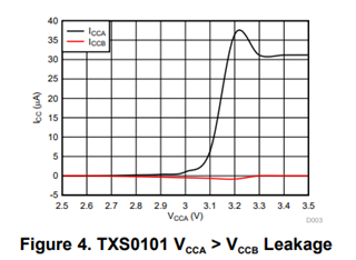
Have port A VDD connected to 3.3V and port B connected to 2.8V. Noticed that the spec says that VCCB >= VCCA. Since that's not the case, the spec is being violated. However, the part seems to be working most of the time. Occasionally, we get a bad I2C write to the downstream device (only one device connected to port B). Any idea why only sporadically we'd be getting a failure and not all the time? Why does the device have this limitation?

  • Hey Rick,

    There is an internal protection diode between VCCA/ VCCB that becomes forward biased when VCCA is larger then VCCB, resulting in increased power consumption and potential damage to the device. Since the device is being used in a manner outside of the datasheet conditions, there isn't a guarantee for when the device will pass or fail. 

    This app note should explain this further in detail: Biasing Requirements for TXS, TXB, and LSF Auto-Bidirectional Translators

    Regards,

    Jack 

  • Jack, 

    Thanks for the quick response. Is it just a protection diode between VCCA and VCCB? The reason I ask is that we are seeing the data be corrupted which leads me to believe that its more than just a diode between VCCA and VCCA pins. I suspect that there's a data path failure for some reason when this spec is violated. Plus, I'm "only" 0.5V over (VCCA = 3.3V and VCCB = 2.8V), so there won't be that much current flowing from VCCA to VCCB plus the downstream device can accept up to 3.6V, so even if VCCB rises a bit due to the diode biasing, it won't be a problem. I know I'm violating the spec, but I want to make sure that before I revise the design that I fully understand the failure. 

    Thanks,
    Rick

  • Hey Rick,

    Yes it is the protection diode that is becoming turned on. The approx. leakage (1 ch. equivalent of the TXS0102) can be found in the app note shared above: 

    With the device currently operating outside the recommended conditions, possible damage may occur to the device similar to the data path failure that is being observed.

    Regards,

    Jack

  • Jack,

    For my circuit, VCCB = 2.8V and VCCA = 3.3V, so a delta of 05.V. Thus, the leakage current should be close to 0V. Even if it was higher (graph peaks at about 38uA), I don't see that this would cause a problem. If I modify the circuit such that VCCB is 3.3V, the design works/no errors, so no damage is being done to the chip. It still seems like there's some other effect of VCCB being less than VCCA (besides the protection diode) that's affecting the data path

  • note that I checked the VCCB voltage and its 0V, so the protection diode doesn't appear to be conducting

  • its 0V as the power switch that turns on this supply is currently turned off. If the protection diode was biased on, the VCCB voltage should have been >0V

  • is there any way that I can have a conversation with the chip designer? We're about to fabricate 50K PCBs and I need to fully understand why the current units are failing. A protection diode between VCCA and VCCB isn't going to cause data corruption. I reworked 5 boards last night to make VCCB = 3.3V (with VCCA at 3.3V) and that resolved the issue (but stresses the camera chip that's only rated to 3.0V) (no I2C failures), so that shows that the device isn't being damaged and VCCB at 2.8V is causing the problem (data corruption). There must be another mechanism (besides the protection diode) that causes data errors when VCCB is 0.5V less than VCCA. We need to know what that is. Please help get this request/resolution expedited.

  • Hey Rick,

    A biasing requirement for this device is to have VCCA < VCCB during normal operation. Since this is not properly followed, the device cannot perform as expected- leading to increase in power consumption and potential damage to VCCB as it sinks in this excessive leakage current. You may be correct here with the additional leakage paths- I will follow up on this and get back to you. In the meantime, can we confirm if the downstream device can handle this increase of leakage current and not damaged?

    Also observe that once the datasheet guidelines were followed with VCCA = VCCB, the device is operating as expected- therefore it seems that the problem can be resolved by following the datasheet guidelines. If not feasible in your system, you may also see the LSF0102 being used in I2C multi-voltage translation applications as shown in this video: Multi-voltage Translation with the LSF Family- that can be used to level shift 3.3V signals to 2.8V (though note that VREFA needs to be at least 0.7V less then VREFB). 

    If it helps, please provide a schematic and waveform of the data corruption you are seeing for further debugging. 

    Regards,

    Jack 

  • Jack,

    Leakage current won't bother the camera module, but will waste some power. The camera is only rated to 3V max which is why I put the level translator in with the B side connected to the 2.8V camera and the 3.3V host and the enable on the A side. I'll capture the waveform tomorrow.  reader_2p0-4p2_pg4.pdf

  • with a protection diode from VCCA to VCCB and VCCB turned off, I expected to see 3.3-.6=2.7V or so on VCCB, but I get 0V. Strange... The main question though is why the data is being corrupted when VCCB is at 2.8V. I hope you can get one of the design engineers to respond.

  • Hey Rick, 

    The schematic seems fine, no immediate concerns from what I see. Looking forward to the waveform captures- I will get back to you on Design's feedback as soon as I get a response. 

    Regards,

    Jack 

  • Hey Rick,

    I will now close this thread as I have followed up offline. 

    Regards,

    Jack