


Part Number: SN74AVCH4T245
Other Parts Discussed in Thread: SN74LVC1G125
Hi,
The customer encountered the following problems in use, please help to solve them.
1. The following SPI interface, one master and two slave, SN74AVCH4T245RSVR output impedance is too high, resulting in the flash output signal cannot be recognized by the MCU.
-
Connect as follows:
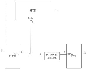
2. In the above connection, the waveform tested at 1 is a square wave with a high level of 1.1V and a low level of 0V. The MCU cannot recognize the high level, so the number read out is usually 0;
The following attempts have been made to no avail;
a. Add pull at place 3 (level conversion input) as shown in the figure above, and the received signal waveform at place 1 is a square wave with a high level of 3.3V and a low level of 2.2V.
b. Add pull at 2 as shown in the figure above, and the received signal waveform at 1 is the same as the initial state, that is, the high level is 1.1V, and the low level is 0V square wave;
c. In the figure above, add the pull down at 3, add the pull at 2, and the received signal waveform at 1 is the same as the initial state, that is, the high level is 1.1V, and the low level is 0V square wave;
If you disconnect cable 3, the communication still cannot be normal. Only by disconnecting cable 4, can the MCU and flash communicate normally.
As above, please help answer, thank you!
