This thread has been locked.

If you have a related question, please click the "Ask a related question" button in the top right corner. The newly created question will be automatically linked to this question.

LSF0102: LSF0102

Part Number: LSF0102
Other Parts Discussed in Thread: LSF0002, LSF0108, LSF0204

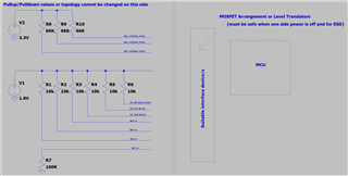
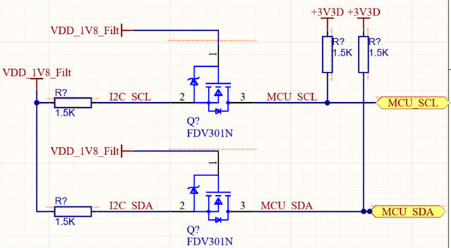
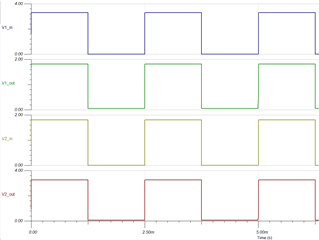
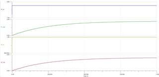
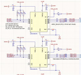
Hi, I am looking for a solution to do a I2C - FAST MODE (400 kHz) Level translation from 1.8V to 3.3V. I have previously used LSF0102, but I cannot use this anymore as on the 1.8V side of the design I have Pull ups of 10kOhms fixed by the Hardware. Please note The Level Translator needs to be fitted on a sub PCB which is connected to the Host PCB using a FPC (a max. of 10pF is expected). The interfacing is shown in the simplified schematic below. The Datasheet for LSF102 discusses Pull up values, which work out to be < 1k. This is not ideal pull up for I2C. Can you advise on this please? Thanks.

  • Hey Billy,

    The LSF0102 can still be used here if we add additional external pullups on the I/Os to effectively lower the pullup resistance (i.e 1.5kohms added to decrease total pullup resistance from 10kohms to 1.3kohms on 1V8 side).

    The external pullup can then be adjusted to meet the VOL requirement of your upstream device as shown in calculation here: I2C Bus Pull-Up Resistor Calculation

    Regards,

    Jack 

  • The examples in the LSF datasheet are not requirements. They use very high pull-up currents that would be needed to reach high speeds. I²C is slow and works fine with weaker pull-ups. 10 kΩ on both sides is a good starting value. If in doubt, check the waveforms with an oscilloscope.

  • Hi Jack,

    thanks for this answer. With your advice I have generated the schematic as per the attached image. I have set the PUs to 1.5 kOhms on both sides. This gives pullup values for 1.8V side of the Hardware (Host Hardware) 1.3 kOhms. On this side I have no idea on the capacitance that each signal is going to see on their path to the Host Processor. On the 3v3 side of the LSF0102 (MCU side) I have set the Pullups to 1.5kOhm (knowing from previous designs 1.8kOhm didn't work properly). On The MCU side I anticipate the track length be about 40 mm (Width 0.2mm; Thickness 0.0175mm; Dk = 4.2) meaning the capacitance on each track + MCU Pins is not more than 20 pF. I hope this should keep the tr < 300ns (In my previous design I couldn't bring the Tr anything less than 460 ns. Couldn't workout why).

    My issue is that I will not have the chance to check the PCB for performance as the PCBs are to be built by the EMS and they will do the checks. Changing the Pullups at their end and check is not possible. Hence I need to get this pull ups correct the 1st time. Can I request you to check and advise me if my schematic would work please?

    Thanks

  • Please note that the pull-ups on both sides act in parallel, so the effect is similar to about 750 Ω. You should not use these example values but much larger values.

    A very rough estimate is about 10 pF per device plus about 1 pF per cm.

  • Hi Clemens, thanks for your reply. I am kind of confused. Are you saying the R on the 1.8V side will be Parallel to the R on the 3.3V side (i.e. for example R12 // R10)? Just noticed that I by mistake connect R11 to SDA as well (it should have been on SCL). So please ignore it.

    Previously I used 2.2k (not exactly this circuit) and I couldn't get the functionality working fine. I had to drop it down to 1.8k. Hence slightly scared of having higher value.

    Any specific values you can suggest?

    Thanks. 

  • @Clements, previously you suggested 10k is a starting point. But that is not a recommended value for Fast I2C right? Please note the Host HW already have a 10k pull up on its Hardware (1.8V side). I put a 1.5k so that I can reduce it to 1.3k as per Jack Guan's comment earlier.

    I am also now thinking why not just use a MOSFET arrangement for translation such as the one below instead. I have previously used this for some low speed applications. Not sure if this would work for I2C Fast Mode. Any comments on this?

  • The LSF has such MOSFETs inside. (These two MOSFETs correspond to the LSF0002; the LSF0102 has an additional biasing circuit to raise the gate voltage to about 0.6 V above Vref_A.)

    When the signal is low, the transistor is on, and all pull-up resistors are connected to the line.

    I do not know how large your bus capacitance is. Check the waveforms with an oscilloscope to see whether the rising edges are too slow.

  • Hey Billy,

    The integrated translators offers a much smaller form factor then discrete options. You may see below app notes/ videos for more info: 

    Integrated vs. Discrete Open Drain Level Translation

    Understanding the pitfalls of discrete level shifting circuits

    Regards,

    Jack

  • Ah OK. I understand. I also wondered of matching of propagation delays etc.. but kind of not too much worried about it because it is not a super speed bus.

    I am thinking the track length on the 3v3 side is about 40 mm. When I did the quick calculation on one of the on-line calculator it gave me a figure of just less than 20 pF. I can add a 2p for the Component pins as well. So this cannot be anything more than 25 pF. On the 1V8 side I am not sure of the value. However I did some measurement on a custom made FPC I have which showed about 4pF. Assuming the Host PCB has 20pF, we can say the capacitance on the 1V8 is also < 25pF. That probably means I can increase the Pull up values to much higher without compromising the tr of < 400 ns (Right?).

    I now understand your point on the equivalent resistance is the parallel combination of the LHS and RHS resistors when pass transistor is on.

    So based on this if I use 4.7k on both sides, I will have:

    on 1.8V side => 10k//4.7k = 3.2kOhm (approx.). I am thinking of a typical I2C fast mode for which I believe the Pullup resistor value range  typically is 2k - 10k (This is just from my memory). Please note the 10k is on the Host PCB side.

    On the 3V3 side => I am planning to include 4.7k as well. This probably is fine for the meeting tr, pull up strength. But it could be a killer for power consumption. Do you think I can fit a 10k instead?

    My issue is I will not have the opportunity to put the scope on the PCB to check this out. This is because the EMS are to build the PCB and they do the bring up. Meaning I will not be able to deal with issues if any very easily. Therefore I must go with the most secure value that will guarantee operation the 1st time. 

    Thanks again for this great support. 

    Regards

  • Hi Bill,

    With 4.7K on both sides (400 KHz input, 25 pF output load), you may expect below (zoomed-out and zoomed-in for your rise time concerns) for 3.3 V input for 1.8 V output and 1.8 V input for 3.3 V output respectively:

    With 10K on both sides (400 KHz input, 25 pF output load), you may expect below (zoomed-out and zoomed-in for your rise time concerns) for 3.3 V input for 1.8 V output and 1.8 V input for 3.3 V output respectively, thanks.

    Best Regards,

    Michael.

  • Hi @jack, thanks for these materials. After reading this and watching the video I have now decided to use TXU0104RUTR for the signals that only require uni-directional translation. On the input side I have 10k Pullups from the Host Hardware. But I can live with that because the internal pull down of 5MOhms of this device's inputs. I would have been nice if these have ESD protection as well so that I can save of adding external TVS as the signals enters my PCB (3V3 Side).  Thanks again for the great support.

  • Hi @Michael, thanks for this very useful traces. Is this this a TINA simulation? Really appreciate this. Thanks again.

  • Hi Billy,

    Yes it is, and happy to help while Jack is out of office at the moment, thanks.

    Best Regards,

    Michael.

  • Hi Michael, thanks. So I am thinking I will stick to 4.kOhm on both side. Its very scary that I won't get to test it and we are going to rely on the EMS to test it out. Hence throwing a lot of questions.

    Thanks again.

    Regards

    Billy

  • Hi @Michael,

     I have now decided to use LSF0204RGYR for its pin count. It looks the same as LSF0102. 3 of these devices been used to handle i2c - fast mode, and a few GPIOs which has Open-Drain and push-pull requirements. Except for the I2c I treat all signals on the 'B' Side as push-pull for saving some power. And also there are slow signals and therefore I guess I don't have to worry about the delay between On-OFF (if any).

    I use 3 of these devices and I think this would be the cost effective solution. I checked your LSF0108 package, which seems a bit expensive and may not be a wise option for finding room for this big chip.

    If this circuit is fine, can you please tell me:

    1. How do I leave the unconnected (unused) bits (A4 - B4). Can I leave them floating?

    2. Do I have to add TVS on the A side as they are connected to an external port. I need to comply to IEC-61000-4-2.? These are unipolar signals.

    Thanks

    Regards

    Billy

  • 1. The LSF is an analog switch; you can leave unused channels open.

    2. The internal ESD protection is designed only for what happens during automated assembly. For external ports, you need more protection.

  • Hi @clemens, Thanks for this. I have added unipolar TVS to the port. Thanks for confirming. On the A side I have current protected all lines so that the MCU is safe when driving LSF0204. I didn't do that on the external component side. I guess it should be fine as the A side are all Open Drain and the current is pulled from the Pull ups.

  • Hey Billy,

    Please let us know if you have any further questions. I will close this thread in the meantime.

    Thanks,

    Jack 

  • Hi Jack, thanks for the great help. This case now been considered as resolved. Regards Billy