LSF0108: Bn output high level is lower than VCCB

Part Number: LSF0108
Other Parts Discussed in Thread: TXU0104, TXU0202

Tool/software:

Hi Team,

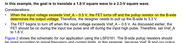
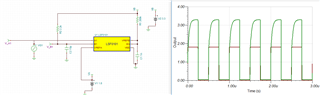
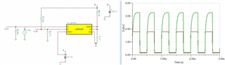
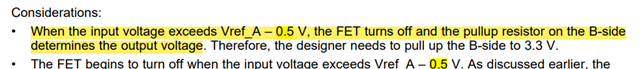
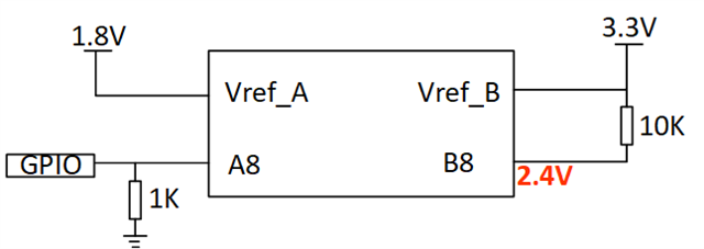
The customer found that when A8 inputs a high level, the high level output by B8 is less than VCCB. Please check the schematic and block diagram below and help analyze the reason? Please note that it seems to be related to the pull-down resistor at A8.

Regards,
Hailiang

  • Hey Hailiang,

    It looks like A1/ B1 are highlighted in the schematic, but A8/ B8 is of concern, can you clarify if that is not the case?

    If so, please remove the 1kohm pulldown resistor on A-side and retest. It is possible that GPIO itself is driving high, but due to 1kohm pulldown, the voltage at A8 is not high enough to switch off the internal FET, therefore B8 is also not as high as VREFB. 

    Regards,
    Jack 

  • Hi Jack,

    In the schematic, It is A8/B8 were highlighted. 

    The customer found that after increasing the pull-down resistor from 1k to 10k, the output voltage of B8 was normal. Can you help analyze the problems caused by the 1k resistor in more detail?

    Also,here is the feedback form customer, could you pls help?

    1, From the datasheet description , if the B-side is high , the switch status should be high impedance , if so, the A-side voltage should be driven by the external pull up, so I can not understand the A-side GPIO driven high by itself , Can you please share the internal switch circuit ? 

    2, The A8 pin was leak from B8 , if the B8 goes to high , how does a-side voltage is clamped at Vref-A ?

    Regards,
    Hailiang

  • The LSF is a passive switch. The pull-down and the pull-up form a voltage divider.

    The LSF makes a direct connection between the A and B pins when the voltage at either pin is low. When both are high, the switch is open, and the pull-up resistors determine the voltage. For this reason, the LSF should never be used with pull-down resistors.

    See [FAQ] How do the LSF translators work?

  • Hi Clemens,

    I see this AN before. *Voltage-Level Translation With the LSF Family (Rev. B)

    The customer tested the voltage level at A8, it is 1.8V. At this time, the FET is turned off. Shouldn't B8 output 3.3V?

    Regards,
    Hailiang

  • Please check the voltages at VREFA and VREFB.

  • Hey Hailiang,

    B8 is expected to output 3.3V if it is pulled up to 3.3V via R2224. Is it populated at the time of testing, and that VREFB is in fact supplied to 3.3V? Are there any internal pulldowns on B8 that are not shown in the schematic as well? 

    Regards,

    Jack 

  • Hi Jack,

    B8 is populated at the time of testing, VREFB is in fact supplied to 3.3V, the VREFA is supplied to 1.8V, and the A8 pin pull high to 1.8V level by host. There is no internal pulldowns on B8. Customer removed the devices connected to the B8, no difference.

    Customer need to have a pull down resistor at A8 to set default low , But the P/D resistor will impact the B8 output. Change the 1K pull-down resistor to 10k, and the voltage of B8 will be normal. After replacing the IC we found no difference.

    Could you please test on EVM and analyze the root cause? 

    Regards,
    Hailiang

  • The voltage at VREFB must not be 3.3 V. You have shown two different schematics, with and without the 200 kΩ resistor. Please state which one corresponds to your actual circuit. (But this is not related to your problem.)

    As I said previously, all resistors on the A8/B8 lines act in parallel, and form a voltage divider. The LSF requires pull-up resistors at all outputs, so it cannot be used with pull-down resistors, and the default state of all signals always is high.

     You can use the LSF for the two bidirectional signals, but for the others, you should use buffered translators like the TXU0104/TXU0202.

  • Hailiang,

    Here is a quick simulation of the result we can expect between having a pulldown resistor at the input vs when it is not populated. 

    No pulldown on A-side:

    10kohm pulldown on A-side:

    1kohm pulldown on A-side:

    With the 1kohm pulldown on input side, we are effectively forming a voltage divider when a logic HIGH is being driven by GPIO signal from A-side. This does not allow the voltage at A1 to be close to VREFA (or 1.8V) so the switch does not fully open and results in B1 not reaching 3.3V. Note that the highlighted paragraph mentions FET turning off, but recall that FETs are analogous in nature, so there is not a certain voltage that the FET turns fully on and fully off. 

    Regards,

    Jack

  • Hi Jack,

    Customer test the voltage at A8 pin, it is 1.71V. And customer want to know the definition of high voltage. Could you pls comments? It seems no data in datasheet, but the description in the AN seems not accurate.

    *Voltage-Level Translation With the LSF Family (Rev. B)

    Regards,

    Hailiang

  • Hey Hailiang,

    This is expected due to the 10kohm pulldown and should not be of concern as the FET is in a semi-open state (we see that output is receiving 3.3V with external pullups installed, which is good). 

    The LSF does not have logic thresholds of its own since it does not have any CMOS architecture within. It only utilizes an internal switch per channel to perform level shift. During operation, the switch closes and bridges the input to the output when the input signal is lower then VREFA, and the switch is open for inputs equal to or greater than VREFA. 

    Regards,

    Jack