This thread has been locked.

If you have a related question, please click the "Ask a related question" button in the top right corner. The newly created question will be automatically linked to this question.

CD4046B: PLL, FM Modulation and Demodulation (Help)

Part Number: CD4046B
Other Parts Discussed in Thread: CD74HC4046A, , SN74LV4046A, MPY634, MPY100

Tool/software:

Hi,

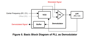
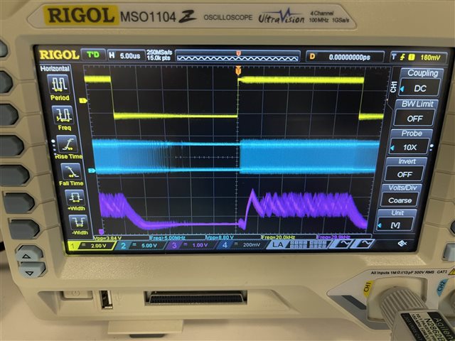
I am a beginner in designing FM Board. My goal is to design a PLL, FM Modulation and Demodulation Board Kit.

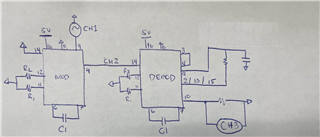
I've read the datasheet and reviewed other designers' circuit diagram. There are some people who provided a schematic diagram for FM Modulation, but upon reviewing the datasheet, it is not explicitly indicated how to design FM Modulation. 

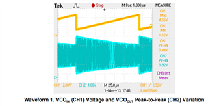
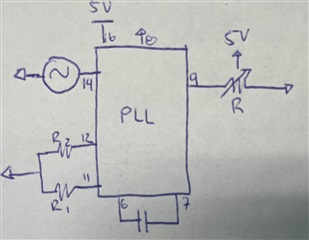
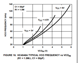
I am also trying to understand how to compute frequency capture and frequency lock range. I think I get the idea for center frequency using the graph, so based on my understanding, if I use 100kOhms on R1 and 470pF, the center frequency is 18kHz. Correct me if I am wrong.

I appreciate if someone can help me.

Thank you in advance. 

  • Hi Patrick, 

    The CD4046B is part of an older device family so unfortunately the design resources are limited. I would recommend checking the product folders for similar devices such as SN74LV4046A and CD74HC4046A and looking through the available datasheets and application notes. Any TI PLL devices that have "4046" in the part name use a very similar architecture so any schematics, reference designs, or application notes you find should be applicable. I've found a few resources that may be helpful:

    How to set up FSK modulation/demodulation using CD74HC4046A: https://www.ti.com/lit/an/slaa618/slaa618.pdf 

    The "Application Information" section of the CD74HC4046A datasheet provides some useful equations, such as how the loop filter components affect the frequency capture range: https://www.ti.com/lit/ds/symlink/cd74hc4046a.pdf 

    Let me know if you have any other questions. 

    Regards, 

    Connor 

  • Hello, 

    Upon reviewing the pdf, and being that the component is a newer model, which I want on my design. I went out with CD74HC4046A. I am still missing key information on my circuit design. 

    Based on these https://www.ti.com/lit/an/slaa618/slaa618.pdf, there are some designators that I am not sure how to use.

    Modulation: TP1

    Demodulation: TP1, TP2, JP1 and JP2

    On Modulation why is VCO out is not attached to COMPin whereas demodulation has a connection I think.

    SIGin is connected to ground in modulation and SIGin is connected to function generator in demodulation, so TP1 in Mod gets the function generator?

    Is there a newer model for 2206CP and 2212CP? 

  • Hi Patrick, 

    Just to confirm, are you referring to Figures 4 and 6 for the modulator/demodulator schematics? 

    "TP" stands for test-point, in the modulator schematic TP1 is used to inject the signal you want to modulate. For example, looking at Waveform 1 the signal on CH1 is would be connected to TP1, and CH2 is measuring the modulated output from the VCO. 

    On the demodulator schematic, TP1 is the modulated input, TP2 is the demodulated output, JP1 selects with phase comparator to use, and JP2 should be shorted to use VCOout as the COMPin input to the phase comparator. 

    The modulator does not need to use the phase comparator at all which is why VCOout is not connected to COMPin. The modulator only requires setting the center frequency of the VCO to the desired carrier frequency, and inputting some data signal into the VCO input voltage. With this setup VCOout will directly output the modulated signal. On the other hand, the demodulator output is essentially a buffered output from the phase comparator. The working principal involves tuning the VCO to the carrier frequency of the modulated input (by using a closed loop PLL with a low pass filter), and detecting the phase difference between the VCO and modulated signal. 

    Let me know if this answers your questions. 

    Regards, 

    Connor 

  • Based on my understanding on what you said, 

    If there is something that I am missing, please let me know.

    I also see that you mentioned tuning with a low pass filter like actively tuning it using variable resistor? 

  • Hi Patrick, 

    Your diagram with the modulator/demodulator connected together looks correct. 

    You could use a variable resistor to tune the VCO, but an RC low pass filter implemented as shown below will cause the VCO frequency to automatically follow the carrier frequency of the modulated input signal. The error signal from the phase comparator passes through the low-pass filter before entering VCOin, so the VCO may not track the modulated input exactly depending on the data rate of the modulated input and bandwidth of the LPF. Let me know if this makes sense. 


    Regards, 

    Connor 

  • I think I understand what you are referring to \the frequency after PC will lean more towards modulated frequency rather than vco-out frequency which ideally supposed to be balance between both. Once the LPF picks up the signal which includes the error, the VCOin could not keep track the modulated signal in the input of the PC's modulated signal. 

    What you are referring to in tuning the VCO? is it R1 of demodulator or R3 of LPF demod?

    Also, on my second circuit for just an individual phase lock loop would it work? my goal there is to show how phase lock loop works, and how it gets lock when frequency of the input change until it locks. 

    Thanks,

    Patrick

  • Hi Patrick, 

    Sorry for the confusion, when I was talking about tuning the VCO I was referring to how the feedback (PC + LPF) will adjust the VCOin voltage of the demodulator until the VCO frequency locks to the carrier frequency of the modulated input. 

    Can you clarify which circuit you're referring to? I'm seeing a circuit with a PLL but it looks like it's just the modulator. 

    Regards, 

    Connor 

  • Hi Connor,

    So the VCOin will be adjust automatically to tune without varying any resistor/capacitor in feedback (PC + LPF)? maybe my conception of tuning is different from yours. If you can enlighten me, that would really help.

    I am referring to this:

    the goal is to make two individual board kit. first board kit is PLL, and the second board kit is FM Mod+Demod

    the first board kit is to find the lock range frequency by adjusting the input signal from low frequency to high frequency, and when it will out locks itself once it reaches the max frequency. 

  • Hi Patrick, 

    That's correct. See the general description on pages 3-5 of the CD74HC4046A datasheet for examples of the behavior of the phase comparator output and VCOin vs. SIGin and COMPin. I've also attached a figure below for reference. Each phase comparator behaves a little differently, but In general the phase comparator will output a high voltage whenever SIGin is leading COMPin, and a low voltage when SIGin lags COMPin. When the phase comparator output is fed through a LPF and into VCOin (i.e. a closed-loop PLL), the feedback will cause the VCO to lock to the input frequency. The capture range and lock time will depend on the passive component values (R1 and C1 to change the VCO center frequency/tuning range, R3 and C2 to change the bandwidth of the LPF). The 4046 PLLs tend to have a very wide tuning range, see the figure of VCO frequency vs. VCOin for an example of what I mean. Does this help, or do you have something else in mind when you refer to tuning the VCO? 

    If your goal is to lock to the input signal, then you should be operating in a closed loop (PCout -> LPF -> VCOin). If you're trying to find the min/max frequency of the VCO (or find a curve of VCO frequency vs. VCOin),  then it would make sense to use a potentiometer to set VCOin manually. 

    Regards, 

    Connor 

  • "passive component values (R1 and C1 to change the VCO center frequency/tuning range, R3 and C2 to change the bandwidth of the LPF)." is the one i have in mind by tuning it cuz if the output is so fast that it does not lock then I need to adjust the frequency using variable resistor and if there's noise on the waveform, tuning it with a variable component which on top of that has already have a good pcb layout can help minimize the noise.

    Upon reviewing the PCs', i only use PC2 or PC3 when I only need fmax or fmin to be demodulated?

    im now calculating the loop filter, but I am not sure if this is right

    I assuming I use PC1 and I have Vcc = 5V, R1= 25K, C1 = 1110pF and Fo = ~100kHz. 

    I will use PC2/3's calculation to get 2FL = ~140kHz

    For LPF, R3 = 25K, 450pF to get ~140kHz. 

    is this something right/wrong or is there better way to do it?

  • Hi Patrick, 

    What frequencies are you planning to use for the center frequency and modulated frequency? Can you use the same values for R1 and C1 on the modulator/demodulator to ensure they have the same min and max frequencies? Keep in mind that in steady state the VCO should lock to the input signal, it's during the transients when the input frequency quickly changes that the VCO takes time to adjust due to the LPF. This is necessary for the phase comparator to generate an error signal which is the demodulated output. 

    I would recommend starting with the passive component values from the "Implementation of FSK Modulation and Demodulation using CD74HC4046A" application note and modify them as needed. For example choosing R1=3k, C1=47pF, R2 = open, E3 = 36k, C2 = 120pF gives a minimum VCO frequency of around 8.2MHz and a max of around 28MHz. The LPF bandwidth is around 36kHz, which is around the fastest modulation frequency that is usable with that particular setup. You'll notice in Waveform 10 that the 40kHz DEMout signal doesn't look very sharp since the LPF is attenuating the rise/fall time. 

    Regards, 

    Connor 

  • I got misconception on the center frequency and fm band. so I tried your example there with exact waveform 10 configurations. My problem that is experiencing is that the demodulated measurement is low than it's supposed to be. is there something that I am doing wrong?

    if I adjust the horizontal scale I can read the 40kHz square wave. 

  • Hi Patrick, 

    Just to confirm, you're saying that you can see the 40kHz square wave on the VCOin but not on DEMout? And this is with the demodulator configuration? 

    Regards, 

    Connor 

  • Yes I can read 40kHz in VCOin:Modulation though it does not match with demodulation. 

    Yellow: Modulation VCOin

    Blue: Modulation VCOout

    Purple: Demodulation

  • That's strange. Do you have the INH pin pulled low? 

    Regards, 

    Connor 

  • Maybe that is the one i am missing. I didn't connect the INH to the ground for both mod and demod.

    The new capture with grounded inh looks like there's resemblance now though it is very noisy. If there's something I am doing wrong, please correct me. 

    If the video doesn't work, here is a youtube uploaded video: https://youtu.be/zhsIhpht-A4

  • I wouldn't expect the DEMout to be so noisy, do you have any low pass filter on the output? Could you also share a schematic or diagram of the setup you are using? It looks like the VCOout is behaving as expected. 

    Regards, 

    Connor 

  • LPF:

    Pin 6 to 7: 47pF

    Pin 9: 122pF to Ground

    Pin 2: R36k to Pin 9

    Pin 10: 50k to GND

    Pin 11: 3k to GND

    Pin 14: SigIn from Mod Pin 4

    Orange Wire: Oscilloscope Channels

    Pin 5 and 8: to GND

    Pin 16: Vcc to Power Supply 5V

    I am not sure if the parasitic capacitance of the breadboard affects that much. 

  • The parasitic capacitance from the breadboard could be making an impact, but since your wiring is fairly short I think the waveforms should be relatively clean. I wonder if some of the noise could be coming through your power rails. What kind of bypass capacitors do you have between VCC and GND? I would recommend having a large cap (maybe around 10uF) on your main VCC/GND rails, and another smaller cap (maybe around 0.1uF) close to the VCC pin of each CD74HC4046. I would also make sure that you have a shared GND between your breadboard, waveform generator, and oscilloscope. 

    Do you also see the same results when you use the other phase comparators? 

    Regards, 

    Connor 

  • Hello Connor,

    I might have figured out the why channel 3 (purple) behaves like that cuz the probe that I am using is very loose and it doesn't clamp nicely. Though there is a lot of noise happening high amplitude at high frequency part of the channel 3. Another thing is channel 2 (blue) it does not truncate the waveform right after at low input. 

  • Hi Patrick, 

    I'm glad to see that you're getting better results now. Your scope might not be accurately measuring the VCO output since the time scale is relatively large (it looks like you're measuring a ~10MHz signal with a timescale of 5us/div, which may work ok with some scopes but not with others). If you need to get a more accurate reading of VCOout you could zoom in your time scale to something more like 100ns/div and try taking single captures right as VCOin is toggling. Another option is to start adjusting the values of the passive components to get the VCO frequency or input modulation frequency closer to the same timescale. 

    It seems like your prototype circuit is functional now, I can go ahead and close this thread unless you have any more questions. 

    Regards, 

    Connor 

  • Ok thanks. Probably one last question? do you have an IC that can handle AM Modulation? I will make a new thread for am modulation. After this question, i think it is okay to close this thread. It wouldn't be removed in the forum right? I can still review our conversation

  • We do have some analog multipliers that could work for AM modulation, see MPY100 and MPY634 as examples. It's also fairly straightforward to create a basic AM modulation circuit using discrete components if you're interested in that. 

    I'll go ahead and mark this thread as resolved, our conversation will still be visible in the forum. 

    Regards, 

    Connor