Tool/software:
Hello,
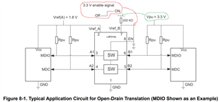
My customer is suggesting the datasheet Figure 8-1 is wrong.
The datasheet 7.3.2 recommends the EN pin to be driven by an open-drain driver.
So, they are mentioning the Figure 8-1 should be the following by right. What does TI think about this?
Best regards,
K.Hirano
The voltage at the EN pin must be lower than 3.3 V; this is usually ensured by the voltage drop over the 200 kΩ resistor. If you were to drive the EN pin high with a push/pull driver, then the voltage indeed would be too high.
The arrows are wrong. When driving the top end of the 200 kΩ resistor to 3.3 V, then the EN pin is at the correct voltage.
Clemens,
Thank you for your response.
Let me ask some more.
Do you mean the 3.3V enable signal in Figure 8-1 is driven from a push/pull driver, not open drain driver?
And the Vref_B is also supplied by the same push/pull driver through 200kohms resister?
Best regards,
K.Hirano
Yes; the external enable signal is connected only to the top of the resistor, i.e., it replaces the 3.3 V supply for the LSF.