This thread has been locked.
If you have a related question, please click the "Ask a related question" button in the top right corner. The newly created question will be automatically linked to this question.
Hi
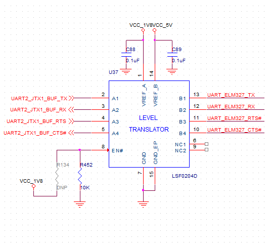
I am using this part LSF0204D for a UART interface (push-pull ) from a SOM from Nvidia JTX1 1.8V to ELM chip 5V side .
In the 1.8 V side since it is push pull i have not used any pull up do we need to use pull up on both sides ?
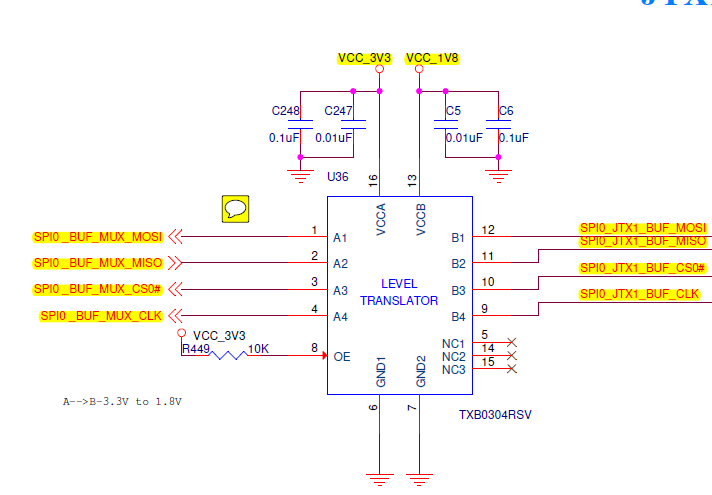
I am using this part TXB0304RSV for a SPI interface (push-pull ) from a SOM from Nvidia JTX1 1.8V to ISP chip 3.3v side .
In the 1.8 V side since it is push pull i have not used any pull up do we need to use pull up on both sides ?
can i use this part LSF0204D for both UART and SPI instead of two separate part ?
SPI max clock from processor is 65Mbps clock 65Mhz
UART from processor 12.5Mbps baurd rate
Second image
If u have any other parts that can be used for both application please suggest
in the data sheet of LSF0204D it is mentioned that
However, if either output is push-pull, data must be unidirectional so it recommends some direction control mechanism to eliminate contention
If so how this part is recommended for SPI interface how to use when both ends are open drain
do i have to pull up to the corresponding voltages in that case ?
TXB0304--This part is more suitable for push pull so shall i use this ?
AGXIN,
I can provide support for the TXB0304. I've notified the applications of the LSF0204 of your request. They will get back to you for that product.
Generally speaking, push-pull interfaces do not require external pullup or pulldown resistors because Logic High and Logic Low levels are driven by the internal PMOS and NMOS transistors of the driver. If there is a situation where the driver is disconnected from the channel (i.e. tri-state), then an external pullup or pulldown resistor would be needed to ensure that the voltage on the channel is at a valid Logic High or Logic Low. Alternatively, you could use a device with 'bus-hold' and avoid the need for those resistors. Back to your application:
TXB0304 requires VCCA <= VCCB, but in your schematic, you've connected VCCA to 3.3V and VCCB to 1.8V.
The SPI CLK from the processor in your application may extend up to 65 MHz (i.e. 130 Mbps). The TXB0304 supports a maximum data rate of 100 Mbps (i.e. 50 MHz clock), and that is with VCCA >= 2.50V. With a 1.8V to 3.3V translation, the maximum support datarate is 60 Mbps (i.e. 30 MHz clock).
My recommendation would be to swtich to the SN74AVC4T774. It supports 1.8V to 3.3V translation and at those voltages, can translate up to 200 Mbps (i.e. 100 MHz clock)
Best Regards,
Nirav
Dear Nirav Patel
Thanks for the reply
But please check the information you have provided on TXB0304 in the datasheet
The supply voltage is mentioned as 0.9 V to 3.6 V in the datasheet
and both ends supports similar voltages so in the schematics that i have shown in the query
I have connected we have used VCCA as 3.3V and VCCB as 1.8V :
as per our operating condition we will be getting a data rate of 140 Mbps
and I have another querry for you that i have mentioned by spi clock frequency is 65mhz how this is equivalent to (i.e 130Mbps ) data rate spi o/p one bit per clock edge (raising or falling) in a MOSI line or a MISO line the data rate is mentioned in the data sheet is for on line in a buffer if so 140Mbps >65Mbps
please let me know how u have taken as 130Mbps ?
Is the data rate mentioned in the datasheet is combined of all the 4-lines or per line data rate ?
Please also check the data sheet you are referring I think u are referring to some different datasheet i am providing the link of the datasheet i am referring from TI
AGXIN,
AGXIN said:But please check the information you have provided on TXB0304 in the datasheet
This was an error on my part. My apologies. I accidentally used the TXB0104 datasheet. The information in your previous post is the correct information.
AGXIN said:and I have another querry for you that i have mentioned by spi clock frequency is 65mhz how this is equivalent to (i.e 130Mbps ) data rate spi o/p one bit per clock edge (raising or falling) in a MOSI line or a MISO line the data rate is mentioned in the data sheet is for on line in a buffer if so 140Mbps >65Mbps
please let me know how u have taken as 130Mbps ?
Bps = Number of data bits per second
Frequency = Number of cycles per second
A clock signal has 2 bits (High Bit and Low Bit) in each cycle
So 65 MHz = 65M cycles/second = (65M cycles/second)*(2 bits/cycle) = 130M (bits/second) = 130 Mbps.
AGXIN said:Is the data rate mentioned in the datasheet is combined of all the 4-lines or per line data rate ?
The data rate mentioned in the datasheet is per channel.
Best Regards,
Nirav
Dear sir
Thanks for the reply
Regarding the data rate as far as SPI protocol is concerned data will be sent on any one of the edges on one line based on the mode we are selecting based on the settings in CPOL and CPHA
so among the four line clock has the highest toggling probability than data (65 Mhz is the highest toggling line i.e clock line )
So if my clock from master is given as 65Mhz under any combination the data rate is less than 65Mbps because i am latching the data only on any one of the edges (you can see the clock wave form is toggling more frequent than the data)
What i understand is in any one of the edge the bit will be present in any one of the line at a given point of time
from the timing diagram you can see that either at the raising edge or at the falling edge data is valid not at both edges
But if it is for other protocols like ddr the data will be present at both the edges so data rate will be twice the clock rate but for SPI how 2 bits per clock?
I am still not getting your point "A clock signal has 2 bits (High Bit and Low Bit) in each cycle"