This thread has been locked.

If you have a related question, please click the "Ask a related question" button in the top right corner. The newly created question will be automatically linked to this question.

SN74LV4046A - Frequency multiplier: settings the parameter, where to start?

Other Parts Discussed in Thread: SN74LV4046APart Number: SN74LV4046A

Application: Frequency multiplier for synchronization

Question type: Development and troubleshooting

Support topic: /Product/Development and troubleshooting/

Description of the problem: Hello

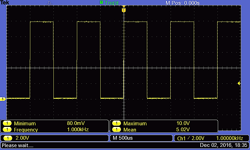
I am designing a frequency multiplier locked to the mains frequency, i.e. 50Hz signal, ideally it shoould lock to the mains frequency f0 and output a frequency f = Mf0, where M is 512 and is obtained with a 4040.
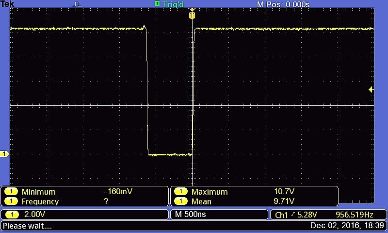
I used to design with older ICs we had in-stock, HCF4046, but the jitter provided of 1us over a period of 39us was way too big for the application.
So I changed for the SN74LV4046, I never used this IC but a colleague of mine told me that the faster logic could be a solution.
Now the problem, if I used the parameters found from the graph for the HCF4046 it does not work and in the datasheet of the SN74LV4046 no graphs are given.
Could you help me?

Please find attached the datasheets.

PS. I wrote also to the TI support but I was guessing that maybe someone else is facing this issue and could find this topic useful.


PLL datasheets.pdf
  • What values did you use?
  • I am using Phase comparator 2.

    Vcc = +5V


    VCO

    C  = 0.5nF

    R1 = 220kOhm

    R2 = 100kOhm

    For a CD4046 it means a range characterized by

    fmin = 20kHz

    f0 = 25kHz (value chosen because the theoretical should be 50*512 = 25600Hz)

    fmax = 30kHz

    NB. this values are not consistent with the range given for the SN74LV4046A (page 13 of the datasheet or 25 of the attached file), but without the graphs I have no idea on how to determine them

    LPF - RC passive filter

    R = 33kOhm

    C = 1uF

    so that I have a cut-off frequency of 5Hz (10% of the input frequency, i.e. 50Hz)

  • Hi Alberto ,

    I appreciate your detailed procedure.

    Although this doesn't reference the SN74LV4046A , I would point out couple of app notes which go in depth along with examples for designing a PLL.

    www.ti.com/.../scha003b.pdf
    www.ti.com/.../scha002a.pdf

    Hope this can help your design.
  • ShreyasRao said:
    Hi Alberto ,

    I appreciate your detailed procedure.

    Although this doesn't reference the SN74LV4046A , I would point out couple of app notes which go in depth along with examples for designing a PLL.

    www.ti.com/.../scha003b.pdf
    www.ti.com/.../scha002a.pdf

    Hope this can help your design.

    Thank you.

    I have already read the application notes, here are the values calculated starting from the graphs and the calculated one

    Calculated accordingly with SCHA003B
    hyp. current mirror such that M = 6.4
    Vcc = +5V
    R1 = 16.8kOhm
    C1 = 10nF
    center frequency = 25kHz

    Calculated starting from the graph
    Vcc = +5V
    R1 = 10kOhm
    C1 = 1.5nF
    center frequency = 25kHz

    The values are very different but, again, the PLL does not lock.

    I'm guessing the problem is in the LPF but, again, I am following the datasheet, here I report the procedure so maybe you can help me find the bug

    divider ratio
    N = 256

    Phase detector 2 gain
    Kd = Vcc/(2*pi) = 5/(2*pi) = 0.8 V/rad (I also tried Kd = Vcc/(4*pi))

    VCO gain
    Ko = 2*pi*(fo - fmin)/(Vcc/2) = 62.8krad/V
    calculated with M  = 6.4 Ko = 66.5krad/V

    wf = (loop frequency)/100 where the loop frequency is 50Hz (the input of the PLL, or should I use 25000 the center of VCO?)
    wn = 8wf
    filter RC time constant t= (KoKd/N)/wn^2

  • Update_

    I have ordered a set of CD4046 just to check if the problem was in the kind of IC. Other than that I found out that the application note at page 19 (see attach below) with an IC HCF4046 show a not constant value on pin 1, while, once that is locked, it should be constant i.e. the VCO oscillating at a fixed frequency.

    I'll let you know what happens with the CD4046BEE4. Otherwise I'll ask some clarifications about the correct setting of the TI's application note

    www.ti.com/.../scha002a.pdf

  • Nothing changes with a different IC.

    In addition, if we consider TI's application note SCHA002 page 19 even with everything equal to TI's layout the output frequency is not stable, i.e. pin 1 is not a constant value as fig.6 page 8 of the same application note of before.

  • Hi Alberto,

    I can understand your frustration with this design - the documentation on LV4046 is significantly lacking.

    Can you grab a scope shot of the SIG_IN and COMP_IN pins when it should be operating and post it up here?

  • Emrys Maier said:

    Hi Alberto,

    I can understand your frustration with this design - the documentation on LV4046 is significantly lacking.

    Can you grab a scope shot of the SIG_IN and COMP_IN pins when it should be operating and post it up here?

    Hi thank you for the interest, before going on with LV4046 (I have ordered a new one on RS since a colleague of mine got all the others burnt in a prototype a multiline clock structure), please have a look at these signal obtained using as a reference the frequency multiplier in the application note scha002a.

    Consider PCP_OUT it should be constant while at every new period of SIG_IN I have a signal of loss of lock (variable in duration, i.e. not at steady state) which is also reflected in VCO_OUT see video.

    While waiting from new LV4046 (hoping that my boss will buy new ones) I am considering TI's CD4046, as far as I know the PCP_OUT should be constant or at least showing a steady-state error, i.e. fixed phase errors between SIG_IN and COMP_IN, not a COMP_IN signal moving around SIG_IN because that means the PLL is not in lock in a stable condition.

    Here is SIG_IN (pin 14)

    Here is COMP_IN (pin 3)

    Here is PCP_OUT (pin1)

    Here is a video of VCO_OUT (pin4).

    Notice that there's a fast flicker in the frequency multiplier output, due to the loss of lock of the PLL see signal at pin1 (figure above)

  • Alberto,

    I just started looking at this also, so forgive my unfamiliarity with this thread.
    Originally you mentioned 50 Hz multiplied by 512 to be 25.6 kHz; Last message shows 1 kHz multiplied by 512 to be 512 kHz.

    As far as I can tell, the loop is locked. PCP_OUT is high almost all the time which means most of the time no correction is needed. However this phase detector only takes action once there is a phase error, otherwise the output is just floating to maintain the status quo. Clearly the VCO voltage will drift a little over time. Once the phase detector sees the drift it produces a 600ns correction pulse indicated by PCPout signal. This correction is not subtle enough so it shows a jump in the oscilloscope display. Probably one jump per correction.

    You could reduce the PC2OUT effect on VCO voltage so that less change per correction pulse occurs. Otherwise chose one of the other phase detectors that output a signal every input cycle. This might spread the jitter out to every pulse instead of widely spaced huge jitter corrections.

  • Thanks for the reply.

    I changed application in order to replicate the application note and check carefully what was going on, that's why I moved to 1kHz rather than 50Hz.

    Now I will try using PC1OUT (pin2) - same conditions as in the application note again to check if something changes, wait for the updates. 

    By the way, I do not understand the reaqson why the proposed LPF has to be changed, after all what I am changing is the phase detector contribution from Vcc/(4*pi) to Vcc/pi.

    Alberto